99.999%
SiO₂ Chemical Purity
1683°C
Thermal Softening Point
±0.02mm
Slot Pitch Precision
1PC
San Diego Custom MOQ
Precision Engineered Catalog
High-Purity Quartz Ware & Wafer Carriers for Precision Processing
Verified dimensional tolerances, thermal stress annealing, and semiconductor-grade synthetic & fused silica assemblies configured for R&D fabs and production lines.
Whitepaper Reference
Material Chemistry, Mechanical Dynamics & Tolerance Thresholds
In high-aspect diffusion furnaces, low-pressure CVD reactors, and advanced acid wet benches, quartz wafer carriers dictate micro-defect yields. Review the baseline physical criteria below.
| Property Parameter | High-Purity Natural Fused Quartz | Synthetic Fused Silica (Direct Synthesis) | San Diego Fab Impact / Significance |
|---|---|---|---|
| Purity (SiO₂ Content) | ≥ 99.995% to 99.999% | ≥ 99.9999% (< 0.1 ppm Fe, Cu, Ni) | Eliminates heavy metal cross-contamination during 1050°C gate oxidation. |
| Coefficient of Thermal Expansion (CTE) | 5.5 × 10⁻⁷ cm/cm·°C (20°C - 320°C) | 5.2 × 10⁻⁷ cm/cm·°C | Exceptional resistance to thermal shock; withstands rapid loading cycles without bowing. |
| Annealing Point / Strain Point | 1140°C / 1070°C | 1180°C / 1100°C | Prevents wafer slot sag and micro-pitch drift in prolonged horizontal furnace runs. |
| Dielectric Constant (at 1 MHz) | 3.75 - 3.80 | 3.70 - 3.75 | Optically neutral; ideal for RF plasma chambers and inductively coupled etch fields. |
| Slot Pitch Machining Tolerance | ±0.05 mm standard; ±0.02 mm precision | ±0.02 mm ultra-precision laser cut | Prevents automatic wafer transfer robot (end-effector) mispicks and particle-shedding micro-scratches. |
| Hydroxyl Content ([OH⁻]) | < 5 ppm to < 30 ppm (Dry grade) | < 1 ppm (Special Plasma) or up to 1000 ppm | Low OH prevents premature high-temperature devitrification into cristobalite. |
Regional Cluster Integration
Precision Quartz Applications Across the Greater San Diego Innovation Hub
From university incubators on Torrey Pines Mesa to compound semiconductor cleanrooms in Sorrento Valley, custom quartz wafer carriers serve specialized clean-tech frontiers.
RF, 5G Wireless & Compound Fabs
San Diego stands as the epicenter of commercial wireless and high-frequency communication ICs. Gallium Nitride (GaN) and Silicon Carbide (SiC) processing require customized vertical and horizontal quartz boats capable of continuous 1150°C rapid thermal annealing without particle contamination.
Next-Gen Microfluidics & BioMEMS
La Jolla and Sorrento Mesa biomedical powerhouses develop high-throughput DNA sequencing chips and diagnostic bio-chips. These processes mandate ultra-flat quartz slide substrates and observation windows with exceptional deep-UV transmission down to 185 nm to ensure optical sensor accuracy.
Defense, Aerospace & Naval Optics
With major defense hubs situated around North Island, Point Loma, and Kearny Mesa, advanced optical systems rely on high-tension fused quartz tubing and pressure vessels for high-energy laser optics, thermal imaging pods, and salt-fog-resistant sensory equipment.
Strategic Growth Vectors
Emerging Trends Shaping San Diego's Advanced Materials Procurement
Market realities in Southern California drive procurement specialists away from standard off-the-shelf components toward specialized, agile fabrication partners.
Rapid Prototype Iteration Over High-Volume Stock
Unlike massive multi-thousand-wafer production facilities in Arizona or Texas, San Diego's fab landscape is distinctively agile. Incubator labs and specialty cleanrooms iterate new wafer geometries (e.g., 50mm, 76mm, 100mm, and non-standard substrate thicknesses for research). Suppliers must provide flexible 1-piece custom batching rather than enforcing high MOQ barriers.
Strict Sub-PPM Chemical Audit Compliance
As microfluidic sequencing flow cells integrate directly with silicon architectures, trace alkaline contaminants (Na, K, Li) cause ionic drift while heavy metals (Fe, Cu) spoil enzymatic fluorescence. San Diego buyers require verifiable spectroscopic assay data, certified acid-bath decontaminations, and cleanroom vacuum packaging prior to shipment.
Direct Manufacturer Advantage
Engineering Precision Rooted in Donghai's Crystal Heart
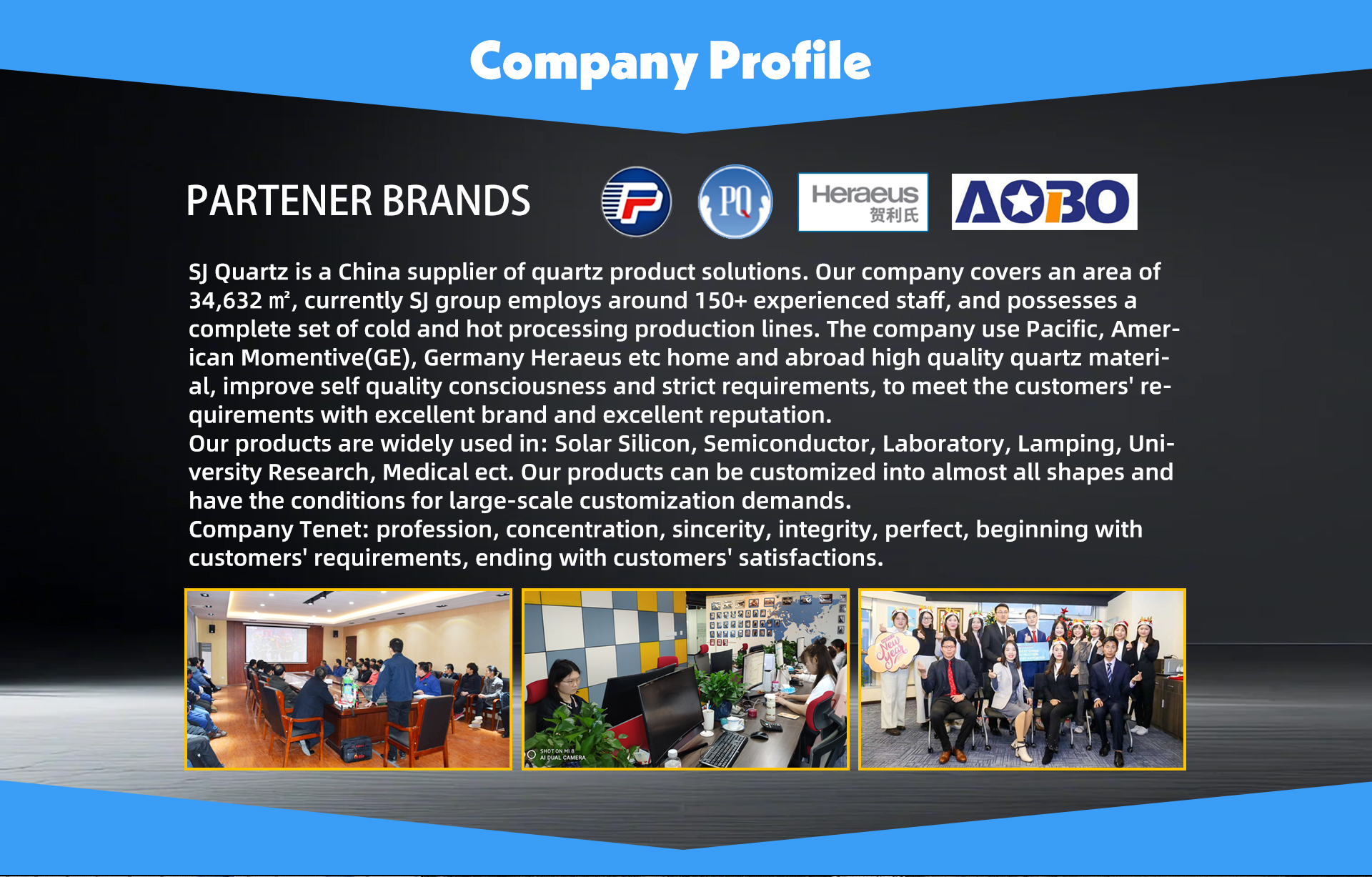
Headquartered in the Jiangsu Donghai Economic Development Zone—the global hub of natural high-purity quartz reserves—Lianyungang Vulra Quartz Products Co., Ltd. offers direct-from-source pricing, stringent metalloid controls, and custom glassworking without broker markups.
- TÜV Rheinland Assessed & Authenticated: Full manufacturer audit validating physical production facilities, raw crystal stocks, and automated precision hot-and-cold processing lines.
- Full Thermal Stress Annealing: High-temperature programmable cycle furnaces eliminate residual birefringence and slot-welding micro-strains, ensuring carriers do not warp under cyclic furnace ramp-rates.
- Drawing-Based OEM/ODM From 1 Piece: Send 2D CAD files (.dwg/.dxf) or 3D STEP files; our engineers calculate slot clearance, wafer center of gravity, and chemical resistance profiles before torch touches quartz.
- Global Shock-Proof Packaging: Multi-layer PE film wrapping, custom high-density foam isolation molds, and reinforced export-grade wooden crating prevent freight attrition across trans-Pacific air and ocean routes.
Procurement Intelligence
Frequently Asked Questions: Sourcing Quartz Wafer Carriers in San Diego
Direct technical guidance on material selection, freight handling, import protocols, and slot geometry tolerance specifications.
What is the typical lead time for custom-slotted quartz wafer carriers shipped to Southern California?
For custom engineering prototypes (1–5 pieces), technical drawing review and CNC slotting take 7–12 working days. Expedited air transit via DHL or FedEx to San Diego International Airport (SAN) typically takes 3–5 business days, delivering your carrier in under three weeks total.
How do you guarantee slot pitch accuracy to prevent automated end-effector robot crashes?
We deploy high-precision multi-axis diamond cutting arrays cooled with ultra-pure filtered water. Every wafer boat undergoes non-contact optical video coordinate measuring (CMM) to ensure pitch spacing adheres to ±0.02 mm, complying with SEMI standards for automated cassette transfer.
Natural fused quartz vs. synthetic silica: which material should our lab specify?
For standard high-temperature oxidation, LPCVD, and diffusion up to 1150°C, natural fused quartz (99.995%+) provides optimal thermal stability and structural rigidity at a lower cost. For deep-UV lithography masks or extreme-sensitivity compound semiconductor processes, synthetic silica is recommended due to virtually non-detectable heavy metal levels (< 0.1 ppm).
How do your export shipping protocols mitigate transit shock across long distances?
Fragile quartz assemblies are individually cleaned, wrapped in cleanroom anti-static foil, and cushioned within customized high-density polyethylene form-cut foam blocks. The assemblies are then housed in multi-wall shock-dampening corrugated boxes and packed inside palletized plywood crates with internal tilt/impact indicators.
Can you manufacture legacy or non-standard substrate carriers for university labs?
Yes. We regularly supply custom carriers for 2-inch, 3-inch, and 100mm wafers, as well as rectangular slide carriers, sapphire substrate holders, and custom-angled boats designed for unique R&D plasma immersion or vertical tube configurations. Minimum order quantity starts at just 1 unit.
What post-weld processing is applied to avoid premature cristobalite devitrification?
All quartz wafer boats undergo secondary annealing in programmable electric furnaces to relieve torch-induced mechanical stresses. They are then subjected to controlled hydrofluoric (HF) acid etching to strip volatile particulate micro-debris, followed by DI water cascading rinses to yield a pristine, chemically stable surface.
Accelerate Your San Diego Fab & Cleanroom Pipeline
Access our comprehensive high-purity quartz product catalog, submit CAD drawings for instant manufacturability assessment, or consult directly with our senior quartz glass technicians.