Process Chamber Viewport Windows
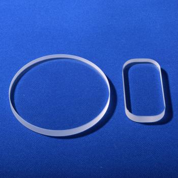
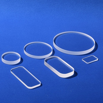
Optically polished parallel discs for pyrometry, laser endpoint detection, and visual inspection.
Learn More
In modern high-density wafer fabrication, advanced sub-7nm lithography, and 3D NAND vertical gate architectures, contamination margins are calculated at the parts-per-billion (ppb) scale. In this operating envelope, Semiconductor Grade Quartz Glass serves as an indispensable baseline material. Vitreous fused silica offers near-zero thermal expansion (5.5 × 10⁻⁷ /°C), unmatched thermal shock resistance across 1100°C gradients, superior dielectric isolation, and inert chemical stability against aggressive halogen process gases including NF₃, CF₄, and anhydrous HCl.
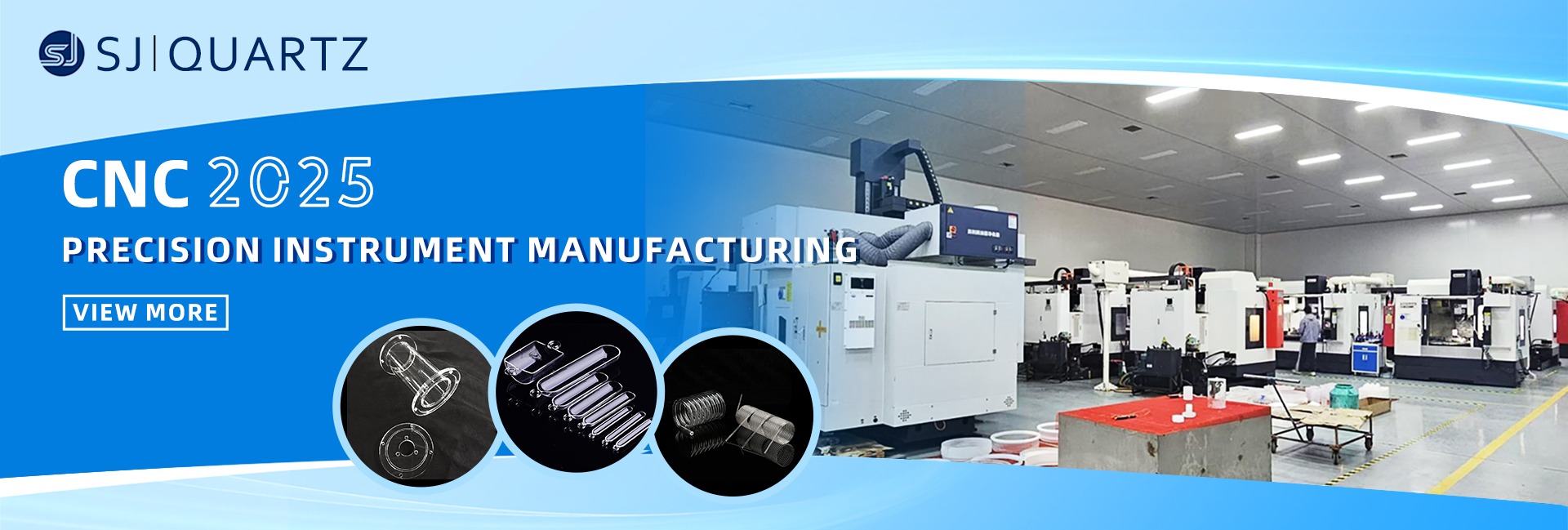
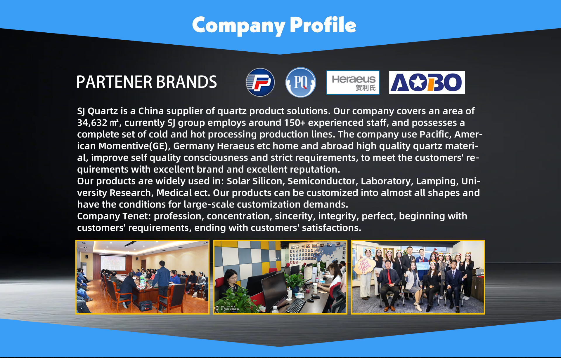
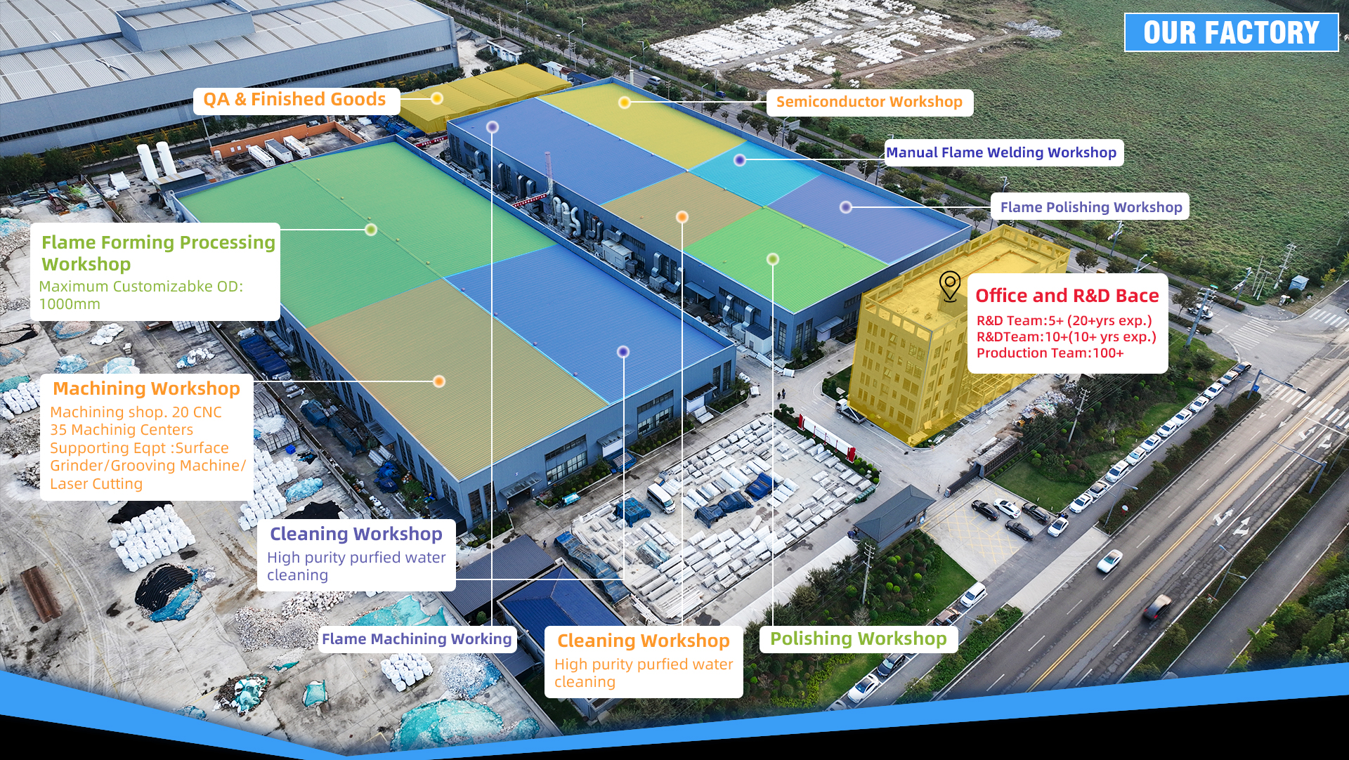
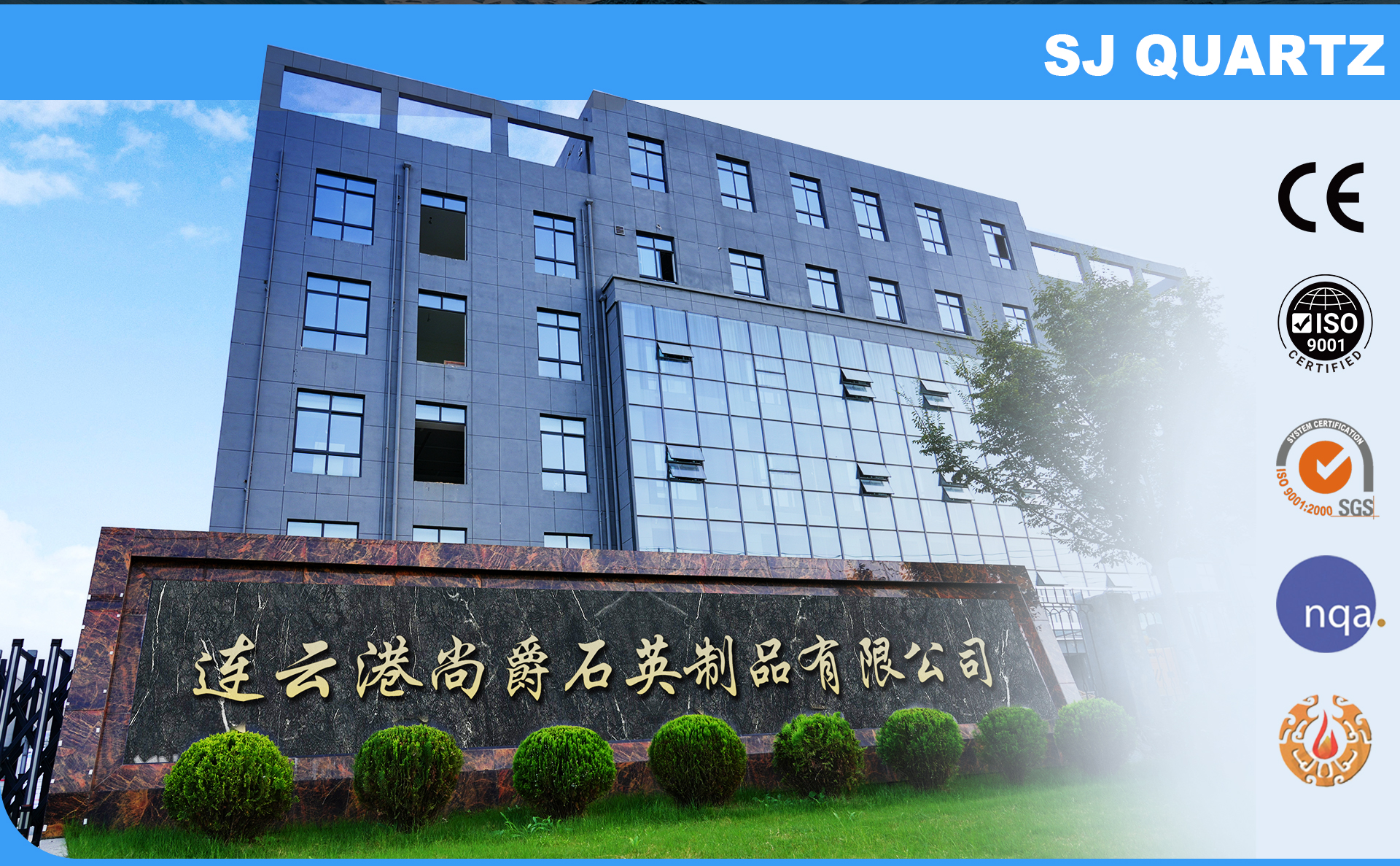
Lianyungang Vulra Quartz Products Co., Ltd. is a verified custom manufacturer operating in Donghai County, China—globally acknowledged as the epicentre of high-purity natural silica sand processing. Operating direct from No. 9, Dingxin Road within the Jiangsu Donghai Economic Development Zone, we engineer mission-critical fused quartz components tailored for wafer handling, vertical diffusion furnaces, epitaxial growth injectors, and plasma etch chambers. Our metallurgical purification regimes and thermal vacuum annealing lines prevent thermal lattice collapse and control volatile alkali-metal outgassing (Na, K, Li), safeguarding semiconductor yields against gate-oxide breakdown and lethal lattice defect propagation.
Whether configuring high-aspect vertical quartz boats, high-flow chemical vapour deposition (LPCVD) process liners, or custom focus rings with sub-10 μm dimensional runout, our precision engineers support global semiconductor fabs, university nano-centers, and lithography tool makers from 1-piece custom prototyping to recurring fab consumable replenishment contracts.
Alkali elements (Li, Na, K) and transition metals (Fe, Cu, Ni, Cr) are strictly suppressed to mitigate deep-level trap formation within silicon substrates.
With an annealing point at 1140°C and softening point reaching 1683°C, components prevent structural sag across continuous 1100°C furnace campaigns.
Engineered stoichiometry resists halogen (F, Cl) plasma attack in reactive-ion etching (RIE) reactors, reducing particle shedding and wafer defects.
Desilanol thermal processing keeps OH content below 30 ppm, preserving structural viscosity, reducing devitrification kinetics, and ensuring vacuum integrity.

As wafer fabs scale up worldwide and next-generation packaging accelerates, procurement teams must balance tighter purity requirements with global supply continuity. Here is how the procurement ecosystem for semiconductor grade quartz glass is evolving.
The industry-wide shift toward large-diameter 300mm (12-inch) wafers has elevated mechanical demands on quartz process tubes and carriers. Tube outer diameters exceeding 450mm to 800mm must maintain tight dimensional circularity, precise wall-thickness uniformity (±0.2mm), and resistance to gravitational sag during long-duration vertical furnace cycles. Sourcing teams are consolidating supplier rosters around manufacturers possessing high-tonnage electric melting capabilities and large-swing glassworking lathes.
Geopolitical concentration in raw high-purity quartz (HPQ) sand reserves has underscored the strategic need for raw material diversity. Procurement directors at Tier-1 fabs are auditing suppliers based on upstream mineral security. Donghai-based processors with access to purified natural crystalline deposits have emerged as resilient alternative hubs, shielding buyers from raw material allocation bottlenecks and long delivery backlogs.
Leading fabs increasingly assess quartzware using Total Cost of Ownership (TCO) models rather than piece-part pricing alone. Premature quartz failures cause costly chamber downtime, lost wafer batches, and extensive recalibrations. Procurement directives now prioritize vendors that execute automated CNC 5-axis machining, controlled hydrogen-oxygen flame sealing, Class 1000 cleanroom chemical etching (HF/HNO₃ de-ironing), and multi-layer vacuum bagging.
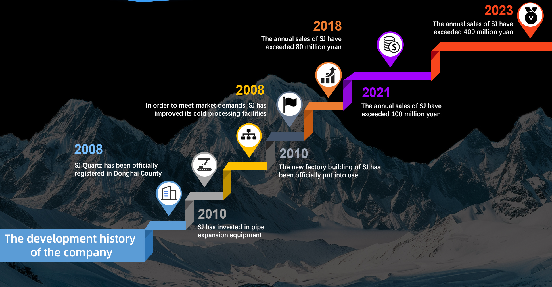
From early commercial glass melting to atomic-precision synthetic vitreous silica, key technical milestones demonstrate how modern quartz meets sub-micron semiconductor fabrication standards.
Electro-fusion of natural quartz sands provided first-generation thermal tubes with fundamental 99.99% SiO₂ matrix purity.
Vacuum desilanol techniques reduced OH radical concentrations below 30 ppm, sharply decreasing thermal sag in diffusion furnaces.
Chemical beneficiation and acid purification eliminated mobile alkali and transition elements down to parts-per-billion levels.
SiCl₄ combustion introduced metal-free, bubble-free fused silica engineered for EUV/DUV optics and advanced photomasks.
Rare-earth doped and composite microstructures prevent micro-cracking and material recession inside high-density plasma chambers.
Semiconductor yields depend on absolute predictability. Compare our verified chemical trace profile and thermo-mechanical properties against international fab operating standards.
| Silicon Dioxide (SiO₂) | ≥ 99.999% (5N) |
|---|---|
| Aluminum (Al) | ≤ 8.0 – 14.0 ppm |
| Iron (Fe) | ≤ 0.1 – 0.2 ppm |
| Sodium (Na) | ≤ 0.1 ppm |
| Potassium (K) | ≤ 0.1 ppm |
| Lithium (Li) | ≤ 0.1 ppm |
| Calcium (Ca) | ≤ 0.4 ppm |
| Copper (Cu) | ≤ 0.05 ppm |
| Hydroxyl Content (OH⁻) | < 30 ppm (Standard) / < 5 ppm (Vacuum) |
| Thermal Expansion (0–300°C) | 5.5 × 10⁻⁷ cm/cm °C |
 SEMI S2 Standards Compliant


Every semiconductor quartz component passes through a rigorous manufacturing chain designed to eliminate micro-cracking, internal stress, and particulate contamination before final deployment.
High-temperature flame welding and flange fusion with zero mechanical micro-cracking.
Sub-micron edge profiling, slotted slotting, and ultra-smooth beveling to prevent thermal chipping.
Surface roughness Ra < 0.5 nm and parallelism < 2 arcsec for optical inspection windows.
Controlled cool-down cycles eliminate residual birefringence and structural tensile stress.
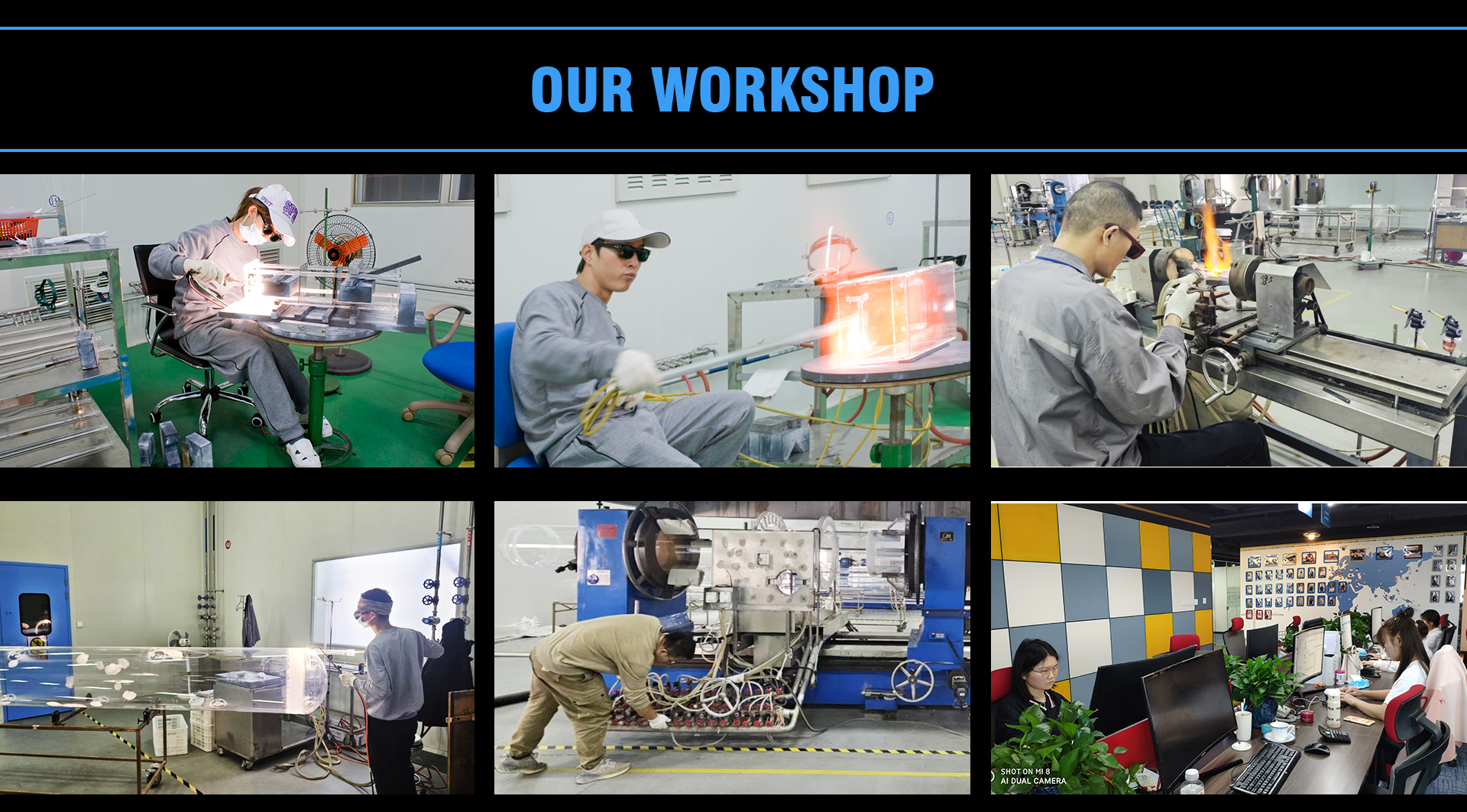
Multi-stage ultrasonic HF/HNO₃ acid bath immersion followed by 18.2 MΩ·cm DI water cascading.
Strict laser coordinate verification, spectrophotometer transmission, and bubble grading.
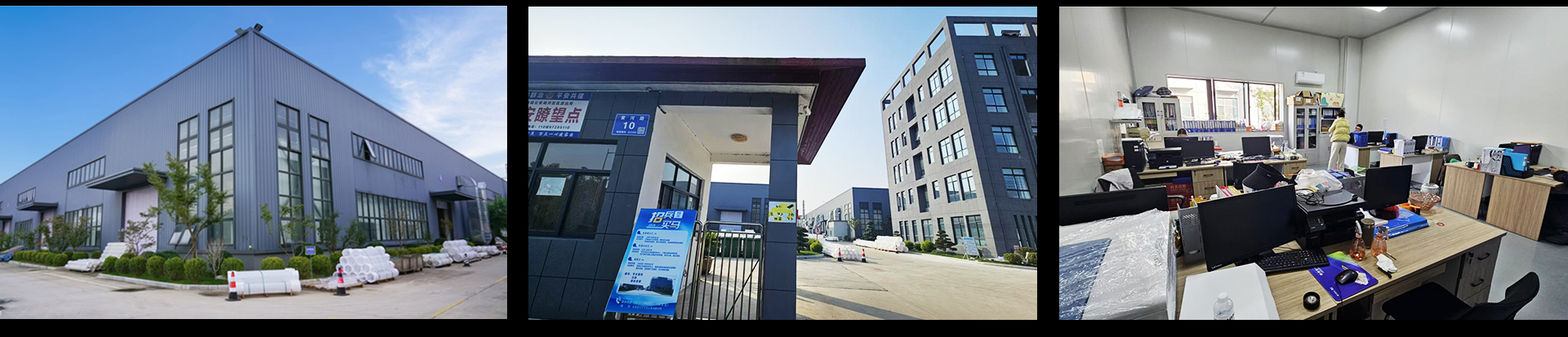
When you partner with Vulra Quartz, you engage directly with a specialized custom manufacturing plant, bypassing intermediary trading margins and communication delays.
Explore high-temperature furnace tubes, precision wafer carriers, and vacuum-sealed quartzware engineered to rigorous front-end fab tolerances.
Every component is manufactured from certified high-purity natural quartz crystal sand or synthetic silica precursors, adhering to precise geometric tolerances.
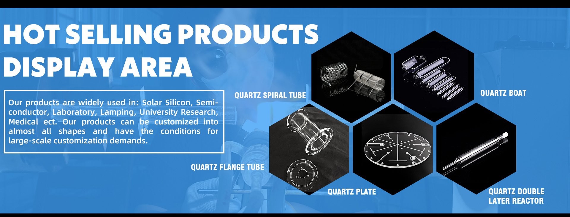
Optically polished parallel discs for pyrometry, laser endpoint detection, and visual inspection.
Learn More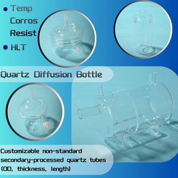
High-purity liquid source delivery vessels and bubblers for ALD and metal-organic precursor vaporisation.
Learn More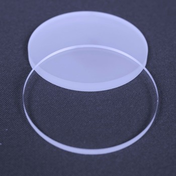
Precision-cut crystallographic orientations for X-ray diffraction, thin-film stress analysis, and ellipsometry.
Learn More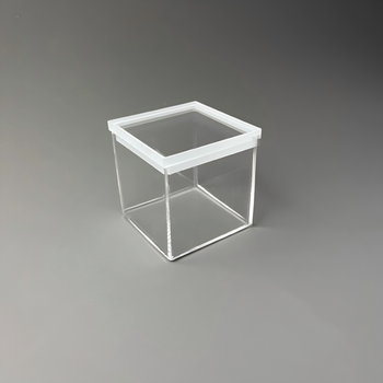
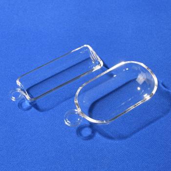
Hermetically sealed reaction cells for copper interconnect electro-plating bath characterisation.
Learn More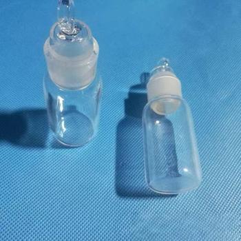
High-temperature, halogen-resistant quartz furnace liners and baffles with 99.999% trace elemental purity.
Learn More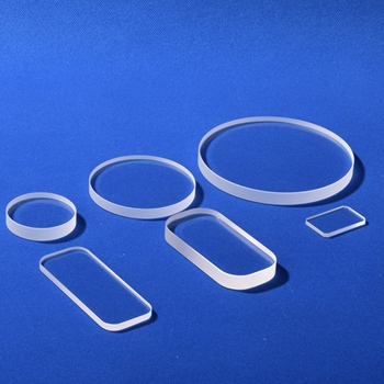
Deep-UV transmitting fused quartz substrates with low bubble inclusion (Class 0) and high mechanical stiffness.
Learn More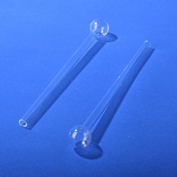
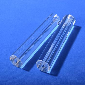
Precision bore 6mm, 9mm, and 12mm stems for high-temperature surface-area and pore-size analysis of fab catalysts.
View in Showroom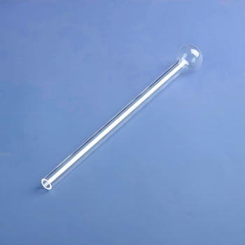
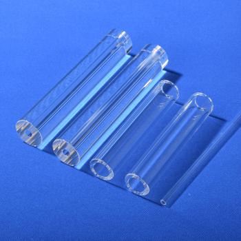
Precision hot-formed curved quartz tubing and laser-perforated orifices for balanced CVD process gas dispersion.
View in Showroom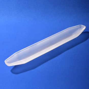
Precision slotted teeth for 100mm, 150mm, and 200mm wafers; zero slot-pitch variation prevents wafer pinch.
View in Showroom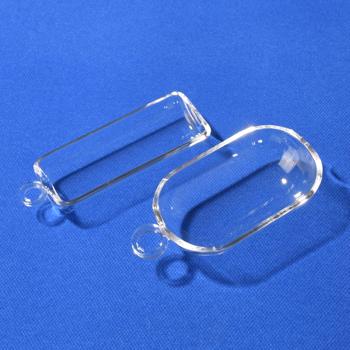
Flat-bottom stable profile designed for horizontal diffusion tubes, rapid thermal ramp-up, and chemical inertness.
View in Showroom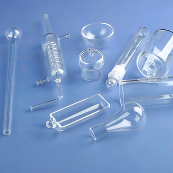
Multi-disk welded thermal radiation barriers preventing furnace end heat loss and maintaining flat temperature profiles.
Learn MoreOur experienced semiconductor glass engineers review your 2D/3D CAD drawings for thermal stress and manufacturing feasibility.
Inquire NowReal-world engineering answers compiled to resolve the technical and operational questions semiconductor procurement teams face daily.
Inquire NowCommercial quartz allows metallic impurities in the range of 15 to 30 ppm and lacks stringent OH radical controls. Semiconductor grade quartz glass mandates total metallic impurities below 5 ppm (frequently reaching 99.999% or 5N purity), with alkali metals like Sodium, Potassium, and Lithium tightly restricted under 0.1 ppm to avoid gate-oxide breakdown and severe wafer cross-contamination at high thermal budgets.
At temperatures between 950°C and 1150°C, mobile ionic species such as Na+ and K+ possess elevated diffusion coefficients inside the vitreous silica network. They migrate out of the quartz vessel wall into the process chamber atmosphere, incorporating into the growing gate dielectric and creating threshold voltage shifts, increased flat-band voltage hysteresis, and dielectric breakdown.
Natural fused quartz is synthesized by electro-fusion or oxy-hydrogen fusion of high-purity natural silica sand. It retains superior structural viscosity and refractory creep resistance at high temperatures, making it the premier choice for structural furnace tubes, wafer boats, and carrier paddles. Synthetic fused silica, created from vapor-phase chemical precursors (e.g., SiCl₄), achieves near-zero metallic impurities (parts per billion) and isotropic deep-UV optical transmission, making it indispensable for photolithography mask blanks and plasma etching focus rings.
Hydroxyl groups terminate the continuous silicon-oxygen tetrahedral networks into non-bridging silanol groups (Si-OH), substantially reducing vitreous glass viscosity and softening point. Under continuous wafer runs exceeding 1000°C, high-OH quartz suffers rapid thermal creep and sagging under load. Lianyungang Vulra Quartz utilizes specialized thermal vacuum desilanol processing to control OH below 30 ppm, maximizing tube dimensional stability.
Devitrification typically nucleates at quartz boundaries when exposed to surface contaminants (fingerprints, dust, alkali salts) in the 1000°C to 1200°C thermal envelope. As high-temperature beta-cristobalite converts to alpha-cristobalite during cool-down below 270°C, a 4.9% volume contraction creates severe micro-fracturing and structural breakage. Robust HF/HNO₃ acid etching, ultra-pure water ultrasonic rinsing, and cleanroom handling prior to loading are mandatory to extend operational lifespans.
Yes. Lianyungang Vulra Quartz is a verified custom manufacturer offering comprehensive CNC cold machining, grinding, laser inspection, ultrasonic drilling, flame welding, and cleanroom annealing. We support precision fabrication from single prototype pieces (1 pc MOQ) up to volume fab supply contracts with strict CMM and cleanroom certifications.
Send your CAD drawings or technical specifications to [email protected] for prompt engineering evaluation, feasibility review, and factory-direct pricing.