Precision Semiconductor Quartz Components
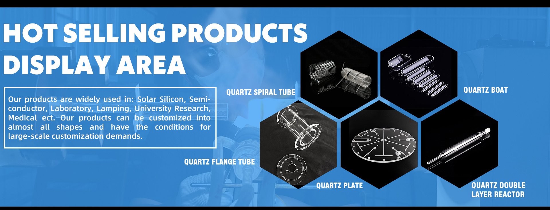
Direct supply from Donghai's world-leading quartz sand hub to Pirkanmaa cleanrooms. Browse our core thermal, optical, and negative-pressure process items below.
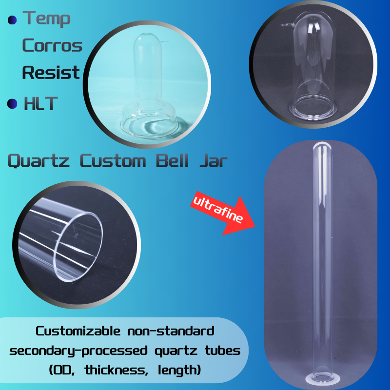
SJ 130 QUARTZ Clear Vacuum Tube 99.99% SiO2 Semiconductor
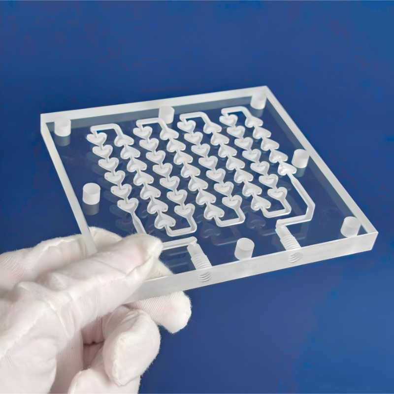
Customized High Thermal Conductance 1750C Circular Quartz Chips
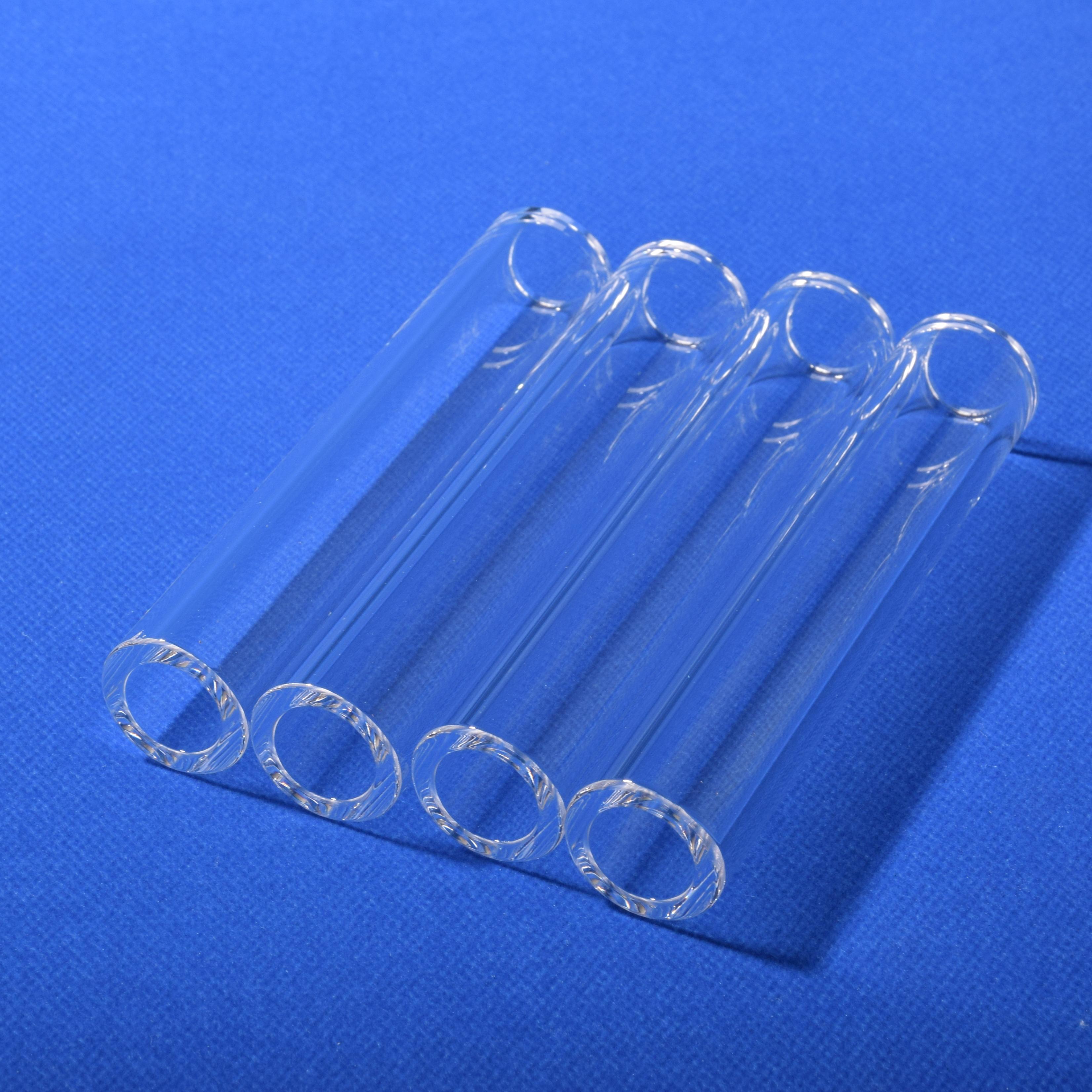
SJ 150 Translucent Oversized Thick Wall Quartz Tube 1100C
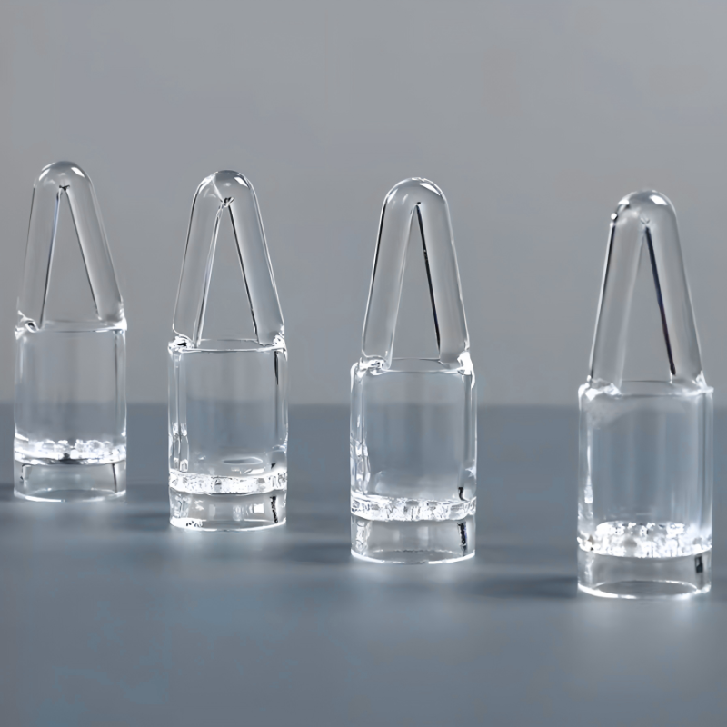
Quartz Crucible Acid/Alkali Resistant Polished Dome Closed End
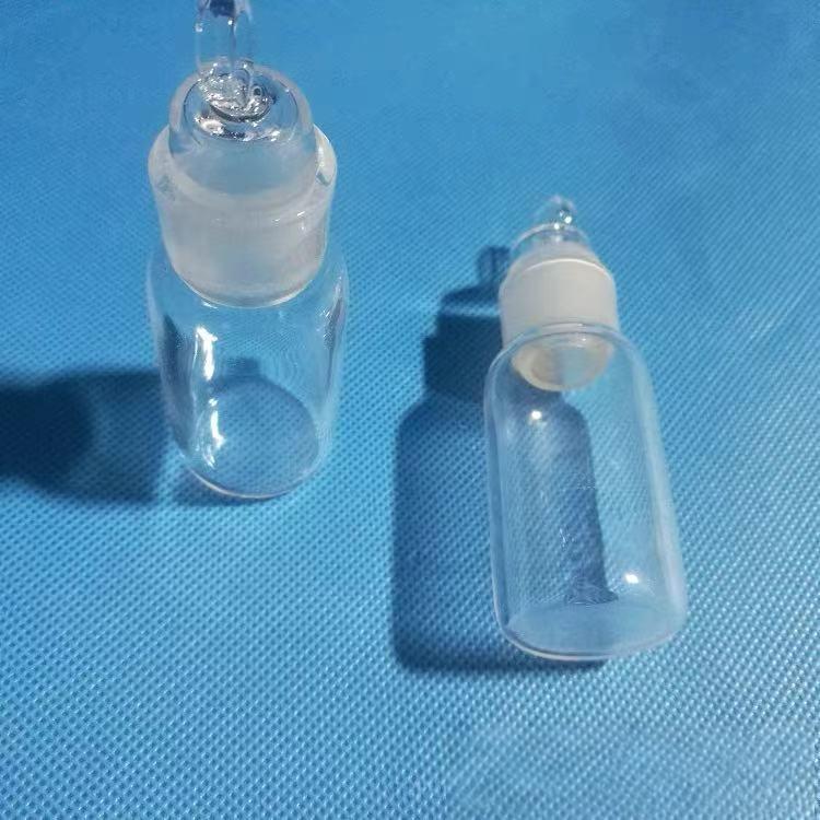
High-Corrosion Resistant Semiconductor 400 Mesh Lab Quartz
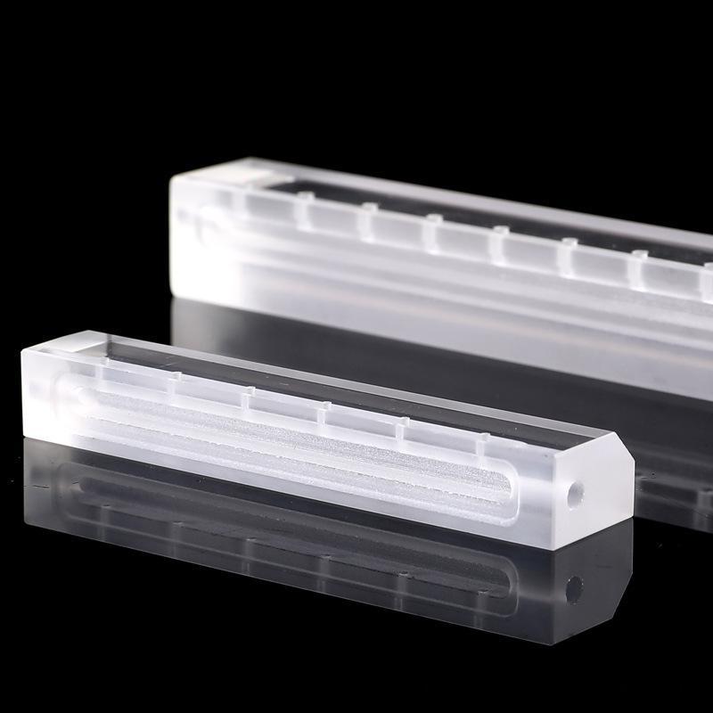
Clear Quartz Testing Sheet Ultra-thin Optical Grade SJ 077
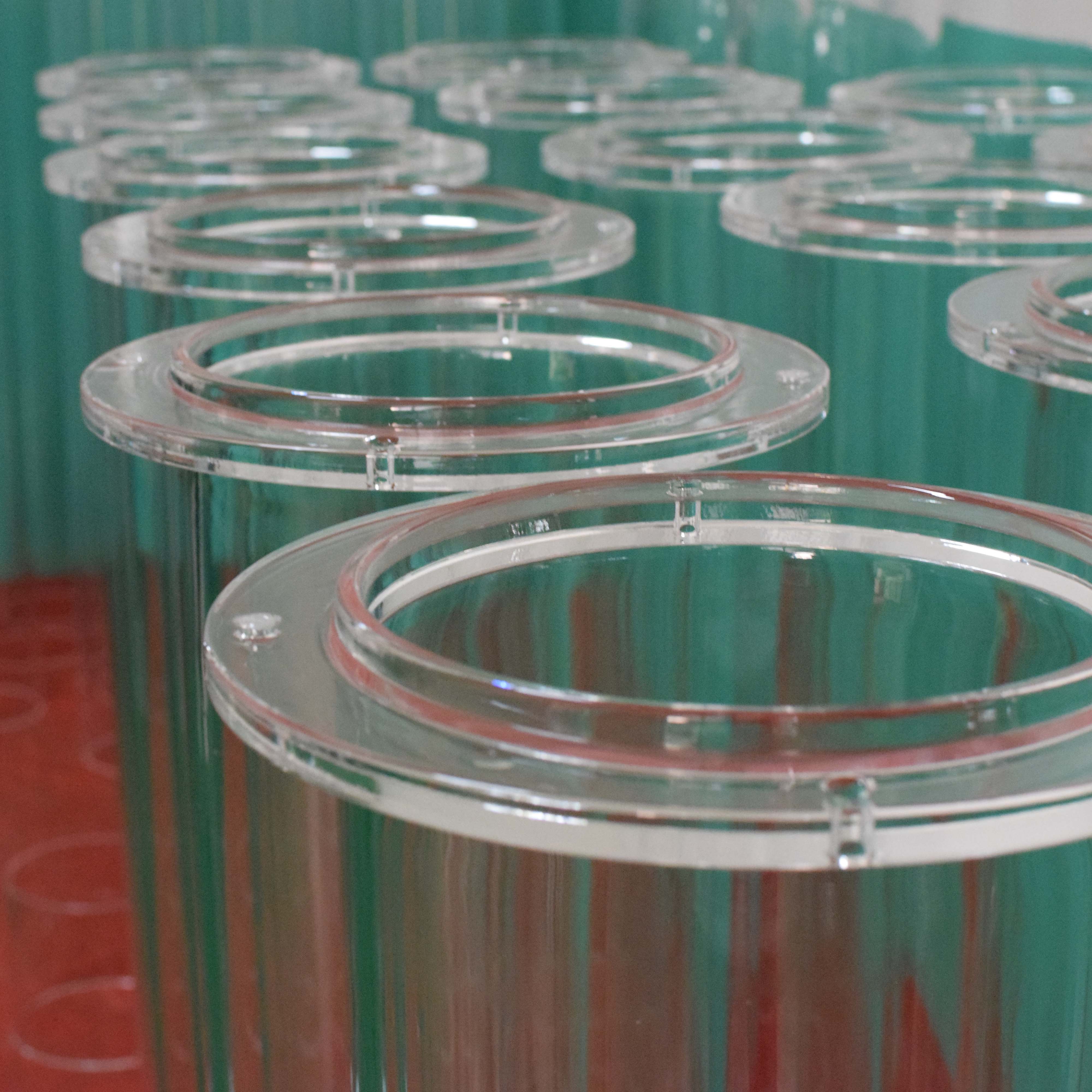
High Purity 99.999% Single Crystal Quartz Tube Flange Re-feeder
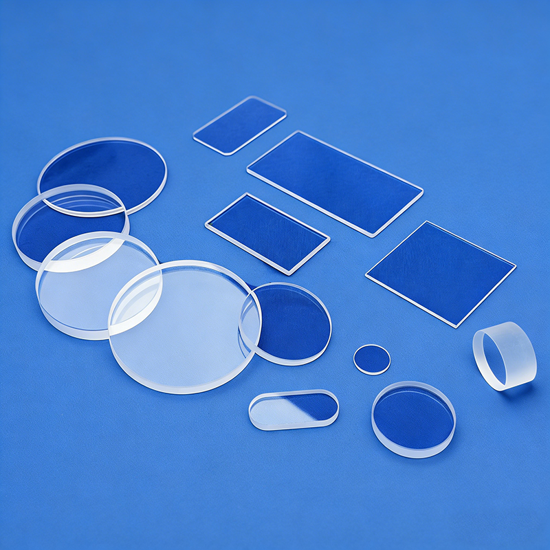
SJ QUARTZ Natural Fused Quartz Arc-Welding Cutting Services
Critical Engineering Demands for Quartz Pedestal Rings in Semiconductor Fabs
In modern single-wafer processing architectures—spanning Atomic Layer Deposition (ALD), Plasma-Enhanced Chemical Vapor Deposition (PECVD), and Reactive Ion Etching (RIE)—the susceptor assembly operates as the definitive mechanical and thermal baseline. Within this critical chamber sub-assembly, the quartz pedestal ring (frequently termed a susceptor focus ring, bottom shadow ring, or wafer edge support ring) carries the rigorous task of defining wafer planarity, managing edge thermal gradients, and insulating electrostatic chuck (ESC) components from corrosive process plasmas.
For semiconductor fabs and advanced research institutes in the Tampere technology hub (Pirkanmaa region), failure to maintain tight dimensional concentricity or trace elemental purity in pedestal rings induces devastating failure modes: premature edge die burnout, local plasma arcing, wafer slippage, and heavy metal cross-contamination. Lianyungang Vulra Quartz Products Co., Ltd. produces customized, drawing-based quartz pedestal rings directly from high-purity natural fused silica or synthetic fused quartz ingots, engineered to withstand aggressive chlorine and fluorine plasmas (CF₄, SF₆, NF₃, Cl₂) at operating temperatures continuously exceeding 1100°C.
- Ultra-Low Metallic Impurities: Iron (Fe) ≤ 0.15 ppm, Copper (Cu) ≤ 0.05 ppm, Sodium (Na) ≤ 0.5 ppm, preventing drift mobility degradation in sensitive III-V and silicon optoelectronic wafers.
- Geometric Precision & Flatness: Total Thickness Variation (TTV) controlled within ≤ 5 μm, with step chamfering down to ±0.01 mm to eliminate wafer edge mechanical chipping.
- Zero-Bubble Ingot Synthesis: Utilizing high-temperature oxy-hydrogen fusion to ensure Class 0 bubble rating within the active wafer-contact zone.
Cold Diamond Machining & Stress-Relieved Annealing Dynamics
Fabricating an ultra-precise quartz pedestal ring requires mastering the delicate balance between brittle material mechanics and thermal shock resilience. Because pedestal rings feature complex geometry—including inner retaining lips, gas purges, lift-pin notches, and counterbored mounting holes—conventional rotary cutting risks introducing subsurface micro-fractures. In our Donghai manufacturing base, all pedestal components undergo cold 5-axis ultrasonic CNC milling with custom diamond-impregnated tooling under flooded deionized cooling.
Following high-precision diamond milling, the components are transferred to our programmable electric annealing furnaces. The structural relaxation cycle ramps to 1180°C and dwells under controlled atmospheres to eliminate all internal mechanical stress vectors induced by machining. Subsequently, a micro-flame or high-purity acid polishing treatment (HF/HNO₃ balance) removes residual micro-cracking, converting the ground silica surface into a smooth, vitreous shield that suppresses particle flaking during thermal expansion cycles inside Tampere ALD reaction chambers.
- Thermal Expansion Coincidence: Linear coefficient of thermal expansion (α) verified at 5.5 × 10⁻⁷ /°C (20°C to 320°C), avoiding thermal mismatch against substrate carriers.
- Surface Micro-Roughness Control: Capable of providing optical fire-polished surfaces (Ra ≤ 0.05 μm) or controlled micro-bead blasted matte finishes (Ra 1.6 – 3.2 μm) to promote polymer/dielectric byproduct adhesion and eliminate chamber flaking.
- CMM Coordinate Verification: 100% full-dimension mapping on 3D Coordinate Measuring Machines prior to cleanroom vacuum double-bagging.
Localized Semiconductor & Photonics Applications in Tampere
The Pirkanmaa region has consolidated its reputation as a global nexus for compound semiconductors, optoelectronics, and nanomanufacturing. Discover how our quartz pedestal rings interface directly with Tampere's industrial requirements.
III-V Photonics & Diode Laser Epitaxy
Tampere's world-leading laser diode clusters around Hervanta require custom susceptor support rings for MOCVD/MOVPE reactors. Our high-purity quartz pedestal rings secure GaAs and InP wafers, preventing parasitic deposition and ensuring radical temperature uniformity across the wafer profile during crystalline growth.
Atomic Layer Deposition (ALD) Reactors
Finland is the birthplace of commercial ALD technology. In high-frequency ALD chambers for thin-film dielectric deposition (Al₂O₃, HfO₂, TiO₂), our pedestal rings act as boundary seals around wafer chucks, preventing precursor back-streaming and protecting sensitive heating platens from corrosive TMA and halide chemistries.
Deep Reactive Ion Etching (DRIE)
In MEMS sensor and optical waveguide fabrication, plasma etching tools rely on our quartz pedestal rings as sacrificial or semi-permanent focus rings. Doped ozone-free or synthetic fused silica options minimize erosion under fluorine RF discharge, ensuring clean anisotropic vertical trench profiles without wafer edge arcing.
Silicon Photonics & Quantum Sensors
Researchers at Tampere University and allied cleanrooms pioneering quantum chips utilize our single-crystal and synthetic fused quartz testing plates and pedestal inserts. Zero-fluorescence, high optical homogeneity, and thermal resilience down to cryogenic interfaces support high-fidelity quantum device packaging.
Comparative Specification Matrix for Pedestal Rings
Evaluating chemical purity, mechanical durability, and thermal tolerances across high-grade natural fused quartz, semiconductor-grade synthetic silica, and standard commercial glass.
| Property / Characteristic | Vulra Semiconductor Grade VQ-999 | High-Purity Natural Fused Quartz | Synthetic Fused Silica (Corning/Heraeus Eq.) | Standard Borosilicate (Reference) |
|---|---|---|---|---|
| SiO₂ Purity Level | ≥ 99.999% | ≥ 99.99% | ≥ 99.9999% | ~ 81% |
| Continuous Operating Temp | 1100 °C | 1050 °C | 1150 °C | 450 °C |
| Thermal Softening Point | 1683 °C | 1665 °C | 1710 °C | 820 °C |
| Thermal Expansion (α) (20-300°C) | 5.5 × 10⁻⁷ K⁻¹ | 5.5 × 10⁻⁷ K⁻¹ | 5.2 × 10⁻⁷ K⁻¹ | 33 × 10⁻⁷ K⁻¹ |
| Fe Impurity (Iron) | < 0.12 ppm | < 0.8 ppm | < 0.01 ppm | > 150 ppm |
| Na + K + Li Impurities | < 0.45 ppm | < 1.8 ppm | < 0.05 ppm | > 40,000 ppm |
| Plasma Erosion Rate (CF₄/O₂) | Low (< 0.18 μm/min) | Standard (< 0.22 μm/min) | Very Low (< 0.14 μm/min) | Rapid Degradation / Slagging |
| Machining Flatness (TTV) | ≤ 0.005 mm | ≤ 0.010 mm | ≤ 0.003 mm | ≤ 0.050 mm |
Semiconductor & Photonics Supply Chain Trends in Tampere
Analyzing key structural shifts influencing high-purity quartz consumables procurement across Finland and the broader Nordic semiconductor corridor.
European Chips Act & Nordic Fab Expansion
With aggressive capital infusion from both Finnish national funding instruments (Business Finland) and EU-level microelectronics sovereignty directives, pilot production lines across Tampere are transitioning toward commercial pilot volume. This demands localized, dependable supply channels for high-wear consumable quartzware like pedestal rings and furnace tubes that bypass European intermediary markups while maintaining audited ISO/TÜV consistency.
Transition to 200mm Wafer Diameters in Compound Fabs
While silicon fabs have long operated on 300mm architectures, compound semiconductor and photonics players in Finland are steadily moving from legacy 75mm/100mm wafers toward 150mm and 200mm substrates. Larger wafer formats exponentially elevate thermal bow risks during CVD and ALD steps. Pedestal rings must possess hyper-flat step margins (<5μm) to guarantee uniform vacuum clamping and prevent wafer cracking.
Rigorous Precursor Purity & Contamination Controls
As device feature sizes shrink in integrated photonics (PICs) and telecom laser diodes, cleanroom managers are implementing trace metal limits below 1 ppb for chuck-adjacent quartz components. Direct sourcing from vertically integrated quartz manufacturers with in-house crystal mining ties—such as Vulra Quartz in Donghai—provides documented spectral purity and batch traceability directly to the melt ingot.
Manufacturing Superiority & Audited Credentialing
Combining Donghai's world-leading natural crystal raw materials with ISO 9001 quality management and third-party on-site verification.
TÜV Rheinland Verified
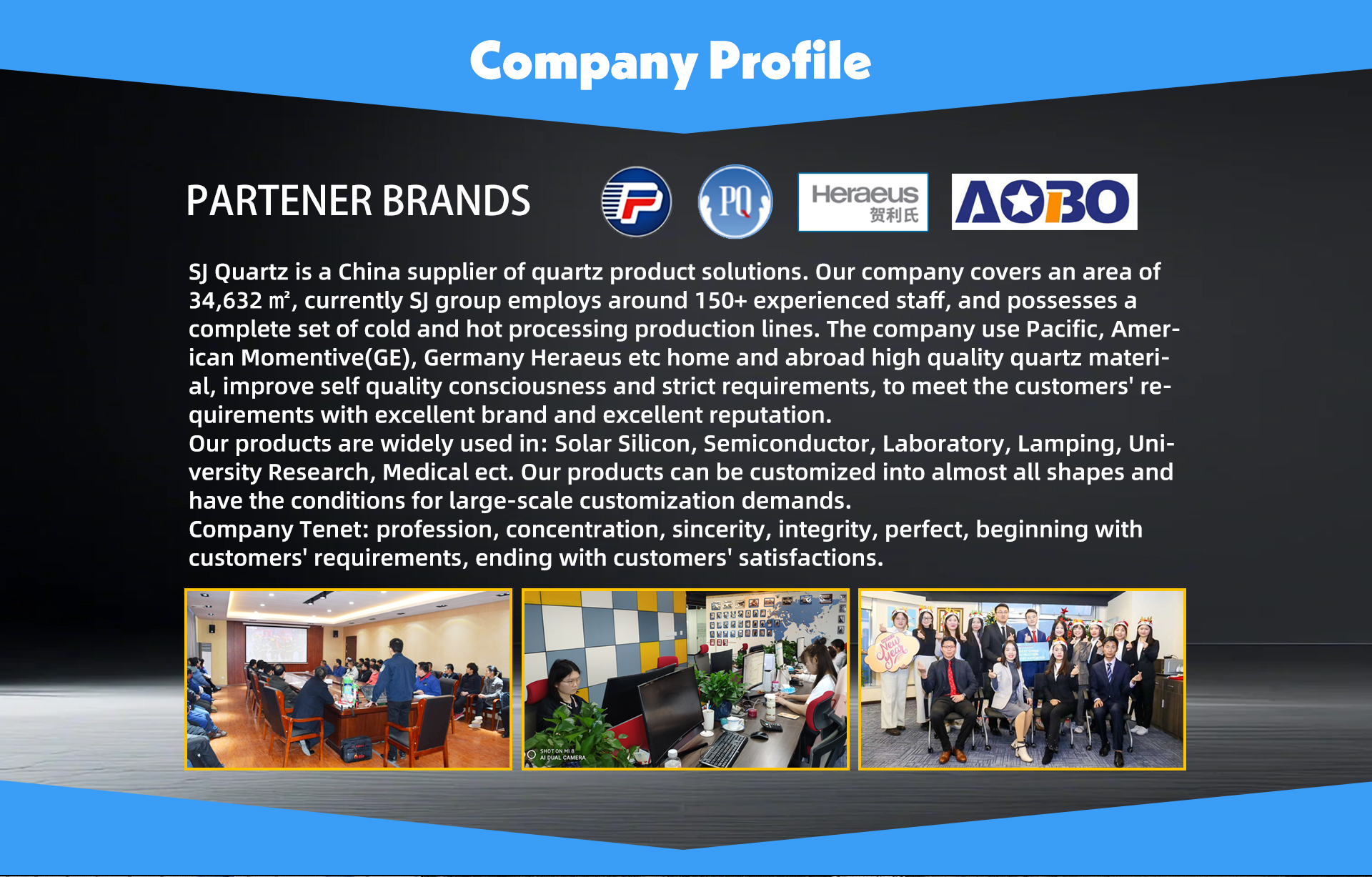
Our physical facility in the Jiangsu Donghai Economic Development Zone is independently inspected and certified by TÜV Rheinland. Legal business operations, manufacturing facilities, and OEM/ODM capacity are authenticated.
Drawing-Based 1-PC Prototypes
We respect the iterative development cycle of Finnish universities and R&D start-ups. We manufacture customized quartz pedestal rings, boats, and vacuum tubes starting from a minimum order quantity (MOQ) of just 1 piece based on CAD/PDF drawings.
Integrated Hot & Cold Working
Under one roof, our shop houses 5-axis CNC diamond grinding, glass lathes, automated hot arc welding, and computerized annealing chambers. This eliminates subcontractor handling and ensures strict control over lead times.
Cleanroom Export Packaging
Quartz pedestal rings undergo multi-stage ultra-pure water ultrasonic cleaning, cleanroom nitrogen blow-down, and double-layer vacuum bagging inside reinforced wooden crates engineered for long-haul air express shipping directly to Tampere-Pirkkala.
Frequently Asked Questions by Tampere Buyers
Practical technical and logistical answers addressed directly by Vulra Quartz's semiconductor tooling engineering team.
How do Vulra quartz pedestal rings resist halogen-based plasma erosion during ALD and dry etching?
Our pedestal rings utilize synthetic fused silica or high-density natural fused quartz with ≥99.999% SiO₂ concentration and negligible micro-porosity (Class 0 bubble distribution). By subjecting the diamond-machined surfaces to proprietary flame-polishing or controlled acid-leaching cycles, we eliminate the micro-fissures and sharp edge lattices where fluorine and chlorine radicals (CF₄, SF₆, Cl₂) typically nucleate corrosive attack. This maintains structural flatness across hundreds of RF plasma hours, preventing localized sheath disruption and edge particle deposition.
What is the standard machining tolerance and Total Thickness Variation (TTV) for custom susceptor rings?
For standard semiconductor tooling orders, we deliver outer and inner diameters within ±0.05 mm, with critical thickness steps held to ±0.01 mm. For high-precision applications—such as edge exclusion rings and electrostatic chuck pedestal covers—our 5-axis ultrasonic CNC machines achieve Total Thickness Variation (TTV) of ≤ 0.005 mm (5 μm) and concentricity within 0.015 mm. Full laser interferometry and 3D CMM inspection sheets are provided with every batch.
What are typical delivery timeframes from Donghai to cleanroom facilities in Tampere or Helsinki?
Standard prototype manufacturing (1 to 5 pieces) typically requires 7 to 12 working days depending on CNC complexity and annealing schedules. Recurring volume production batches run on a 15 to 25-day cycle. For logistics into Finland, express air freight (via DHL, FedEx, or TNT Priority) delivers directly to Tampere-Pirkkala Airport or Helsinki-Vantaa Logistics Hub within 4 to 6 business days. Full customs clearance documentation, HS code optimization, and Certificate of Origin (COO) are managed seamlessly.
Can you manufacture replacement pedestal rings for legacy or discontinued chamber tools (e.g., Applied Materials, Lam, TEL)?
Yes. A substantial portion of our European export service supports legacy fab maintenance and customized OEM tool retrofit. You can supply an original 2D CAD drawing (.DWG, .DXF), a 3D model (.STEP, .IGES), or physically ship a worn/unbroken sample part to our Donghai facility. Our optical coordinate metrology systems reverse-engineer the component, including precise step bevels and underside thermal relief recesses, at a fraction of OEM replacement expense.
How does Vulra prevent particle contamination and packaging damage during international transit?
Every finished quartz pedestal ring undergoes a strict 4-step decontamination process: ultrasonic deionized water wash, hot air drying under HEPA filtration, cleanroom nitrogen blow-down, and double-layer antistatic vacuum sealing. Mechanically, the sealed rings are suspended in high-density customized EPE foam inserts within double-wall corrugated cartons, which are then bolted inside IPPC-certified fumigated plywood export crates. We maintain a zero-breakage track record across long-distance Nordic deliveries.
What metallic impurity limits are guaranteed for your 99.999% semiconductor-grade quartz rings?
Our high-purity natural fused quartz (Grade VQ-999) features total metallic impurities below 10 ppm, with critical cross-contaminants strictly limited: Aluminum (Al) < 5.0 ppm, Calcium (Ca) < 0.4 ppm, Iron (Fe) < 0.15 ppm, Copper (Cu) < 0.05 ppm, Sodium (Na) < 0.5 ppm, and Potassium (K) < 0.5 ppm. For sub-micron gate processes or ultra-clean quantum photonics, we also provide synthetic fused silica where total metallic impurities remain below 0.1 ppm (100 ppb).
Can you provide custom surface finishes like localized sandblasting or optical fire-polishing on the same ring?
Absolutely. Semiconductor process engineers frequently request hybrid surface textures: for instance, high-precision optical fire-polishing along the inner diameter to avoid particle shedding near the wafer bevel, combined with a controlled matte sandblasted finish (Ra 2.0 – 3.0 μm) on the upper perimeter face to anchor dialectic by-product film buildup. Our technicians apply precision masking fixtures during bead-blasting to ensure sharp geometric transitions.
What information is required to receive a formal engineering review and quotation?
To initiate an immediate feasibility review, provide your 2D engineering drawing (specifying dimensions, key tolerances, and surface roughness requirements) or 3D CAD model, along with desired material grade (natural fused quartz vs. synthetic silica), operating temperature, process chemistry (e.g., thermal, plasma, acid), and estimated batch quantities. Our application engineers provide formal quotations and DFM (Design for Manufacturability) feedback within 24 hours.
Accelerate Your Tampere Fab Operations with Precision Quartzware
Whether you require single-piece R&D prototyping for university cleanrooms in Hervanta or scheduled batch supply for industrial photonics manufacturing, Vulra Quartz delivers certified quality directly to your cleanroom dock.
Send an Inquiry