High-Performance Quartz Substrates & Custom Apparatus
Engineered to withstand temperatures up to 1450°C with chemical inertness against aggressive etchants. Explore our core standard and build-to-print fused quartz catalog serving Incheon's engineering base.
Technical Whitepaper: Crystallographic Integrity and Thermal Stability of Quartz Glass Substrates
In high-density microelectronics, wafer-level chip-scale packaging (WLCSP), and bio-photonic analytical instruments, quartz glass substrates serve as the premier foundational medium where conventional borosilicate and aluminosilicate glasses fail. Quartz glass—comprising virtually pure amorphous silicon dioxide (>99.99% to 99.999% SiO²)—exhibits an extraordinarily low coefficient of thermal expansion (CTE) of approximately 5.5 × 10−&sup7;/°C across a continuous operating spectrum from room temperature up to 1100°C. This crystallographic uniformity eliminates thermal-gradient-induced mechanical strain and surface micro-warping, critical metrics for Incheon's packaging cleanrooms that handle sub-micron lithography and extreme ultraviolet (EUV) optical inspection.
As a verified custom manufacturer rooted in Donghai County—the globally recognized epicentre of natural high-purity crystal quartz sand reserves—Vulra Quartz operates end-to-end hot flame forming, automated CNC cold machining, precision double-sided chemical-mechanical polishing (CMP), and vacuum stress-relief annealing furnaces. Our substrate solutions meet the stringent demands of Songdo's leading biopharmaceutical contract development and manufacturing organizations (CDMOs) and the specialized OSAT (Outsourced Semiconductor Assembly and Test) facilities situated across Incheon's industrial axes.
| Physical / Thermal / Optical Metric | Natural Fused Quartz (JGS2 Grade) | Synthetic Fused Silica (JGS1 Grade) | Borosilicate Float Glass (Reference) |
|---|---|---|---|
| Chemical Purity (SiO² Content) | ≥ 99.99% – 99.999% | ≥ 99.9999% (Sub-ppm metallic) | ~ 81% (Contains B²O³, Na²O, Al²O³) |
| Thermal Expansion (CTE: 20°C to 300°C) | 5.5 × 10−&sup7; / °C | 5.2 × 10−&sup7; / °C | 32.5 × 10−&sup7; / °C |
| Continuous Working Temperature | 1100 °C | 1150 °C | ~ 450 °C |
| Softening Point | 1683 °C | 1730 °C | 820 °C |
| DUV Optical Cut-off Wavelength | 220 nm – 260 nm | 170 nm – 185 nm | 320 nm (Opaque to DUV) |
| Dielectric Constant (ε at 1 MHz) | 3.75 – 3.80 | 3.70 – 3.75 | 4.60 – 5.20 |
| Surface Roughness (CMP Polished Ra) | < 0.5 nm (< 5 Å) | < 0.3 nm (< 3 Å) | ~ 1.5 – 3.0 nm |
Precision Applications Across Incheon's Industrial Corridors
Incheon Metropolitan City forms the western technological powerhouse of the Seoul Capital Area, integrating marine clean-energy logistics, world-scale biopharma production, and high-density semiconductor test packaging.
Songdo Bio-Frontier: Biopharmaceutical Synthesis
Home to the world's largest monoclonal antibody manufacturing capacity, Songdo biopharma plants demand optical-grade quartz flow-splitting bottles, photolytic degradation tubes, and high-transmittance flow cells that guarantee zero metal-ion leaching and flawless chemical resistance against aggressive sanitizers and solvents.
Incheon-Namdong OSAT & Glass Core Packaging
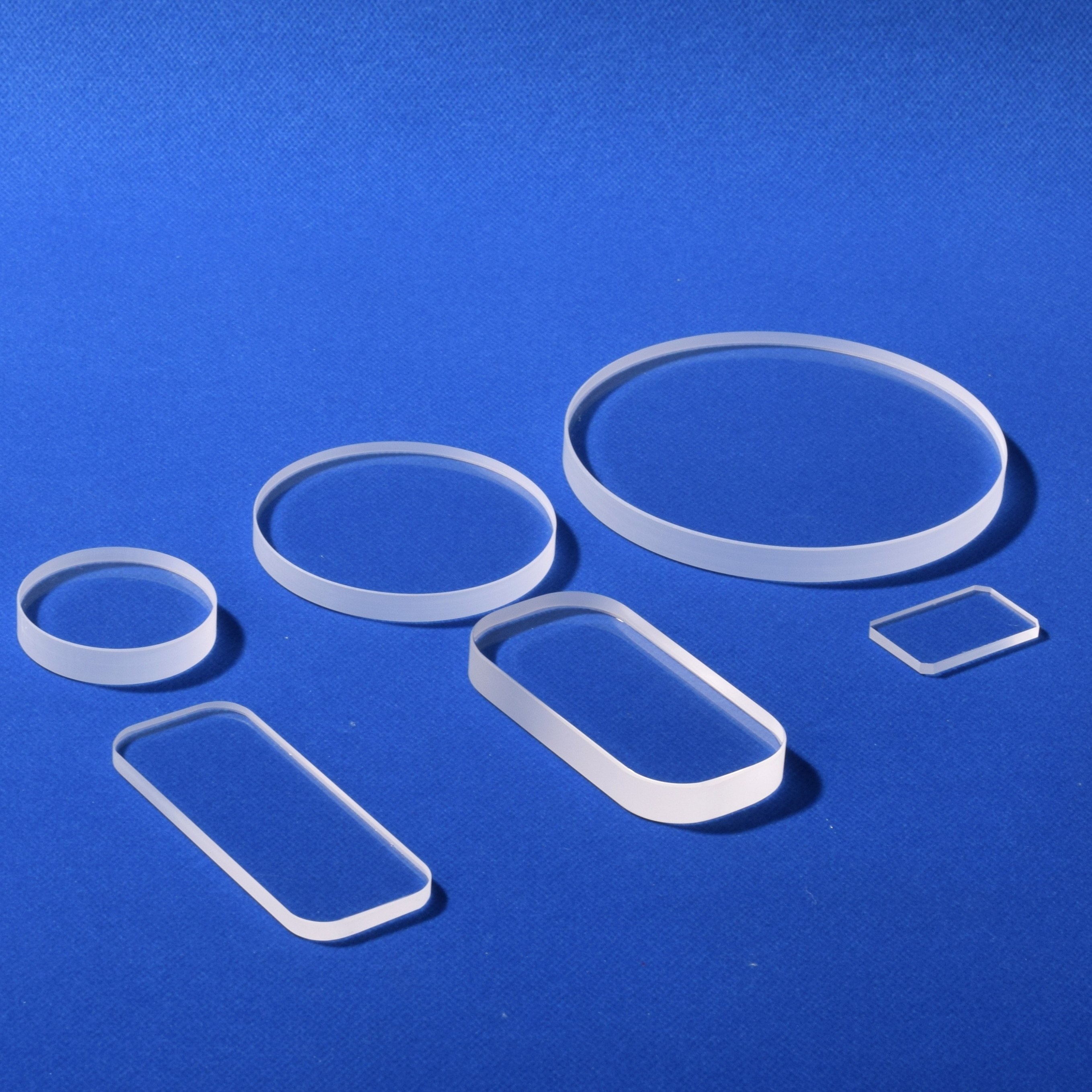
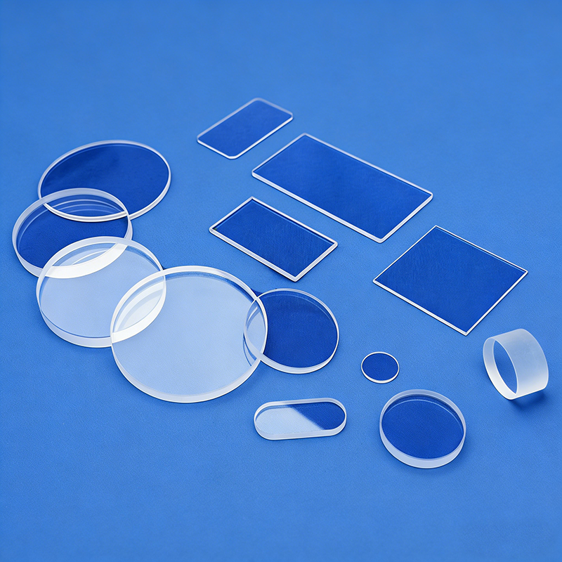
As the microelectronics industry pioneers Glass Core Substrates (GCS) and Fan-Out Panel-Level Packaging (FOPLP) to overcome silicon interposer thermal dissipation limits, Namdong-based semiconductor testing houses deploy our polished ultra-thin quartz glass plates as structural carriers and laser-release carrier substrates.
Incheon Coastal Energy: Photocatalytic Hydrogen
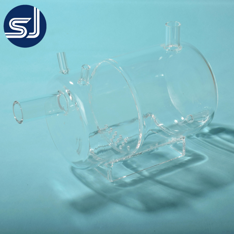
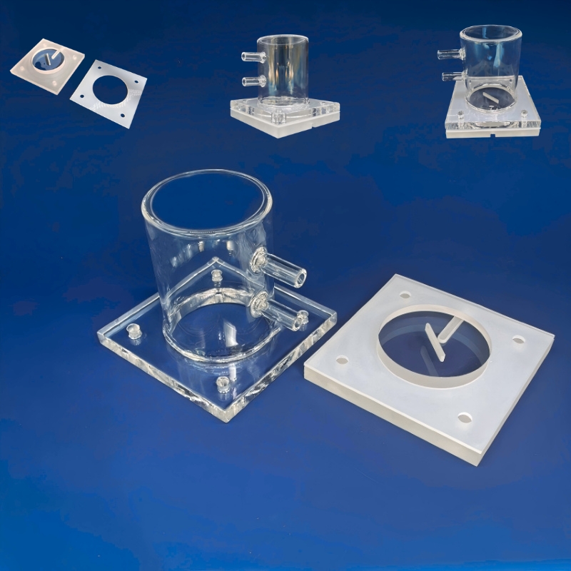
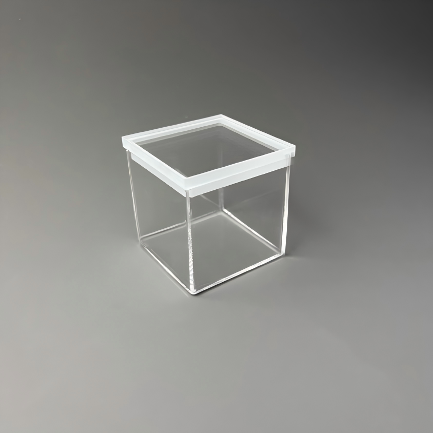
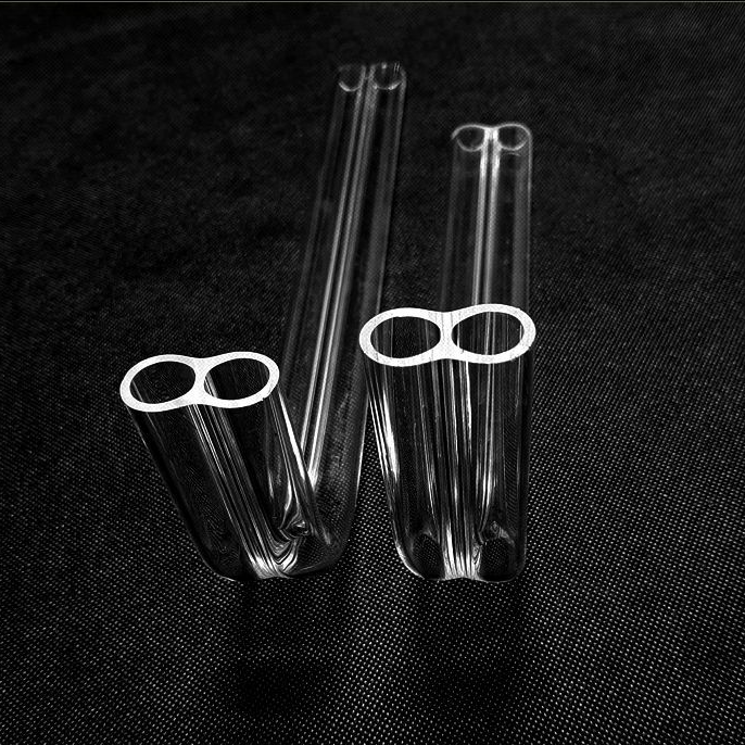
Incheon's specialized hydrogen industrial testbeds utilize our dome-closed electrolytic quartz cells and double-wall tubular reactors. Synthetic quartz and ozone-free fused silica enable 185–254 nm UV light penetration for water-splitting and high-efficiency photo-electrochemical energy conversion research.
Bupyeong & IFEZ Optical Instrumentation
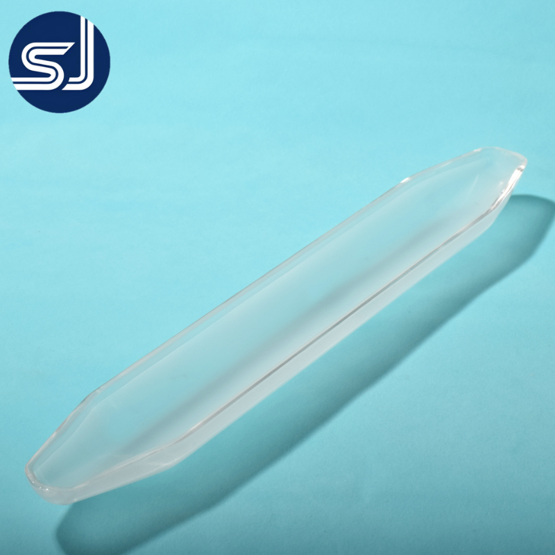
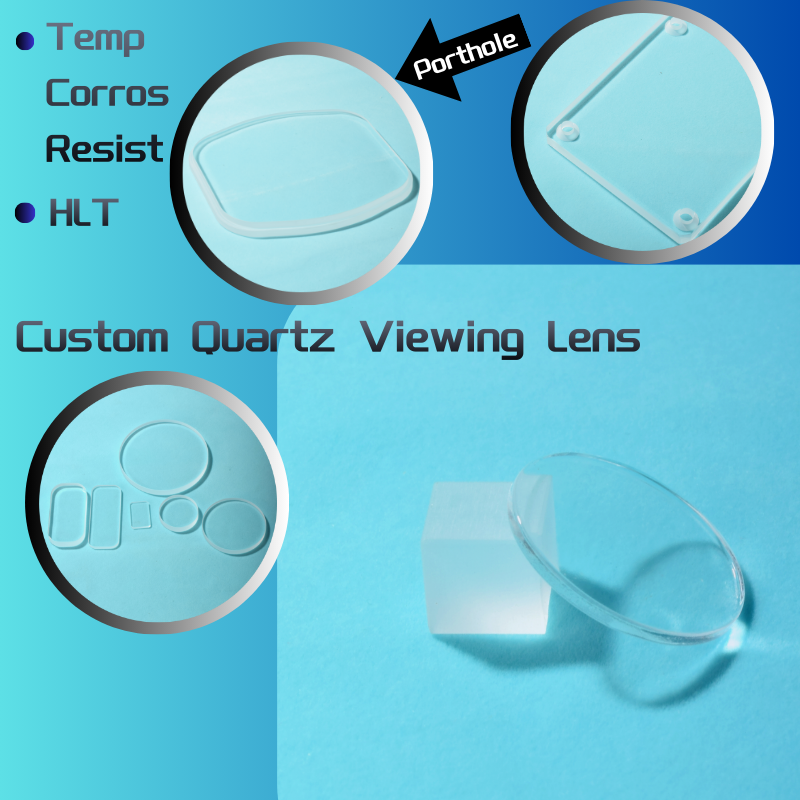
Scientific equipment manufacturers located within the Incheon Free Economic Zone (IFEZ) integrate Vulra Quartz custom-ground observation windows, XRD diffraction sample holders, and precision furnace boats into high-vacuum CVD furnaces, surface area gas-adsorption analyzers, and spectroscopic testing consoles.
South Korea's Substrate Paradigm Shifts: Incheon at the Nexus
Analyzing key structural transformations in advanced electronic materials and how Incheon-based supply chain managers maintain a competitive edge.
Transition to Glass Core Substrates (GCS) in Packaging
Driven by AI processor power densities exceeding 1000W, traditional organic resin substrates suffer from warpage and micro-crack delamination. Incheon's advanced packaging centers are aggressively transitioning to fused silica and quartz glass substrates. With a dielectric loss tangent an order of magnitude lower than conventional laminates and thermal expansion closely matched to silicon (3.2 × 10−&sup6;/°C vs. quartz 0.55 × 10−&sup6;/°C via tailored stress-relief), quartz substrate wafers offer structural rigidity and thermal resistance for multi-die heterogeneous packaging.
Bioprocess Automation & Photonic Monitoring
Songdo's evolution into a global biomedical hub requires continuous, real-time spectrophotometric inline monitoring of bioprocess fluids. Quartz glass substrates and precision quartz flow channels are replacing disposable polymers to eliminate autofluorescence, withstand harsh CIP/SIP (Clean-In-Place / Steam-In-Place) sterilization cycles up to 134°C, and prevent chemical leaching that could adulterate high-value biotherapeutic harvests.
Direct Maritime Supply Chains via Incheon Port
South Korean procurement teams are de-risking single-source domestic intermediaries by contracting directly with upstream quartz manufacturers in Donghai, China. Benefiting from daily container and Ro-Ro ferry links connecting Lianyungang Port directly to Incheon Port (crossing the Yellow Sea in approximately 24 to 36 hours), engineers in Incheon secure custom-machined, cleanroom-ready quartz components at significant cost and lead-time advantages.
Frequently Asked Questions by Incheon Sourcing Engineers
Direct technical and operational answers compiled from our daily collaborations with South Korean manufacturing, QC, and logistics departments.
What is the standard shipping lead time from Lianyungang/Donghai to Incheon Port?
Our manufacturing complex in Donghai is situated less than 80 km from Lianyungang Port. The direct container ferry connects Lianyungang directly to Incheon Port with a maritime transit time of just 24 to 36 hours. For urgent prototyping or low-volume batches, direct air cargo from nearby international airports arrives at Incheon International Airport (ICN) within 24 hours of dispatch, ensuring rapid customs clearance and delivery into Songdo, Namdong, or Cheongna.
How do you prevent micro-cracking and chipping during maritime shipping of fragile quartz?
Every piece undergoes automated ultrasonic DI-water degreasing, cleanroom vacuum sealing with anti-static nitrogen barrier pouches, and suspension packaging inside custom-molded high-density polyethylene (EPE) closed-cell foam buffers. Shipments are consolidated within shock-absorbing export plywood crates equipped with tip-and-tilt and drop-impact indicators, ensuring pristine condition upon arrival at your cleanroom dock.
Do your quartz substrates conform to SEMI standards and Korean RoHS regulations?
Yes. Our quartz substrate wafers and components comply with SEMI standards (M1, M18, and G-series) regarding Total Thickness Variation (TTV < 2 μm), surface bow/warp, and edge exclusion zones. Furthermore, all products are fully compliant with RoHS and REACH regulations, supported by verified TÜV Rheinland inspection audit certificates and batch ICP-MS trace metal impurity reports.
What CAD drawing formats and precision tolerances can Vulra Quartz execute?
Our engineering design department reviews 2D formats (DWG, DXF, PDF) and 3D solids (STEP, IGES, SLDPRT). Using five-axis CNC ultrasonic diamond machining centers, precision wire-saw dicing, and laser cutting, our cold-machining tolerance capabilities reach ±0.01 mm for planar dimensions, ±0.005 mm for substrate thickness, with surface roughness down to Ra < 0.5 nm (CMP optical polish).
When should an Incheon fab choose Synthetic Fused Silica over Natural Fused Quartz?
Choose Natural Fused Quartz (JGS2/JGS3) when your primary application concerns thermal resilience (continuous 1100°C service), furnace carriers, tube apparatus, or standard visible/IR observation windows where budget efficiency is paramount. Opt for Synthetic Fused Silica (JGS1) when operating in the deep UV spectrum (< 260 nm down to 170 nm), when metallic trace impurities must remain below 1 ppm, or for EUV optical masks and laser-induced damage threshold (LIDT) applications.
What is your Minimum Order Quantity (MOQ) for custom-engineered prototypes?
We provide full drawing-based prototyping starting from 1 piece for custom quartz plates, wafer substrates, specialized photoelectrochemical cells, and furnace boats. This enables research laboratories at Inha University, Yonsei Songdo Campus, and fab R&D teams to validate fit, form, and thermal dynamics prior to approving mass production runs.
Why Incheon Advanced Fabs Rely on Vulra Quartz
Combining world-class raw quartz material resources with verified precision cold/hot processing and strict quality assurance systems.
Epicenter of High-Purity Raw Quartz
Situated in Donghai County—known globally as the crystal capital—Vulra Quartz maintains direct provenance over ultra-pure natural silica sand deposits. This upstream advantage guarantees raw batch consistency (>99.999% SiO²) and shields our Incheon partners from international market volatility.
TÜV Rheinland On-Site Assessed
Our manufacturing facility, engineering staff, CNC machining lines, and QA metrology laboratories are fully audited and verified on-site by TÜV Rheinland. We operate authenticated ODM and custom OEM fabrication streams backed by verifiable European CE and RoHS compliance certifications.
Unified Hot-Forming & Cold-CMP Machining
Unlike third-party traders who split orders across fragmented workshops, Vulra Quartz executes tube closing, flame lathe arc-welding, precision core-drilling, CNC edge chamfering, and chemical-mechanical polishing (CMP) under one roof, guaranteeing tight tolerances and predictable delivery schedules.
Vacuum Annealing & Metrology Validation
Every fabricated component undergoes programmed vacuum annealing to eliminate localized internal thermal stress induced during welding. Products undergo laser interferometry, bubble class inspection (DIN 58927), and coordinate measuring machine (CMM) verification prior to final packing.
Connect Directly with Our Quartz Engineering Team
Have a custom substrate drawing, chamber window specification, or specialized reaction vessel project serving the Incheon, Songdo, or Namdong industrial corridor? Upload your design files for a comprehensive technical review, material grade consultation, and factory-direct quotation within 24 hours.