Technical White Paper · Material Science
The Physics of Fused Silica in Sub-7nm Wafer Processing
Within semiconductor and advanced photonics manufacturing, fused silica (vitreous silicon dioxide) represents an irreplaceable structural and process component. Unlike conventional borosilicate or aluminosilicate glasses, synthetic and electric-arc melted fused quartz possesses an ultra-dense, non-crystalline tetrahedral molecular lattice that exhibits an exceptionally low coefficient of thermal expansion (CTE of 5.5 × 10⁻⁷ /°C from 20°C to 320°C).
For fabrication facilities and advanced OEM tooling engineers located throughout the Greater Phoenix corridor—encompassing North Phoenix, Chandler, Tempe, and Scottsdale—thermal stability under aggressive chemical vapor deposition (CVD), rapid thermal processing (RTP), and chlorine/fluorine dry etching is a baseline necessity. Our manufacturing processes eliminate alkali metal contaminants (Na, K, Li) down to single-digit parts per billion (ppb), preventing mobile ion contamination that causes gate oxide breakdown in sub-micron semiconductor devices.
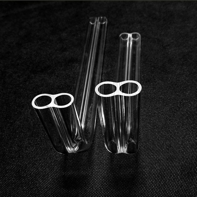
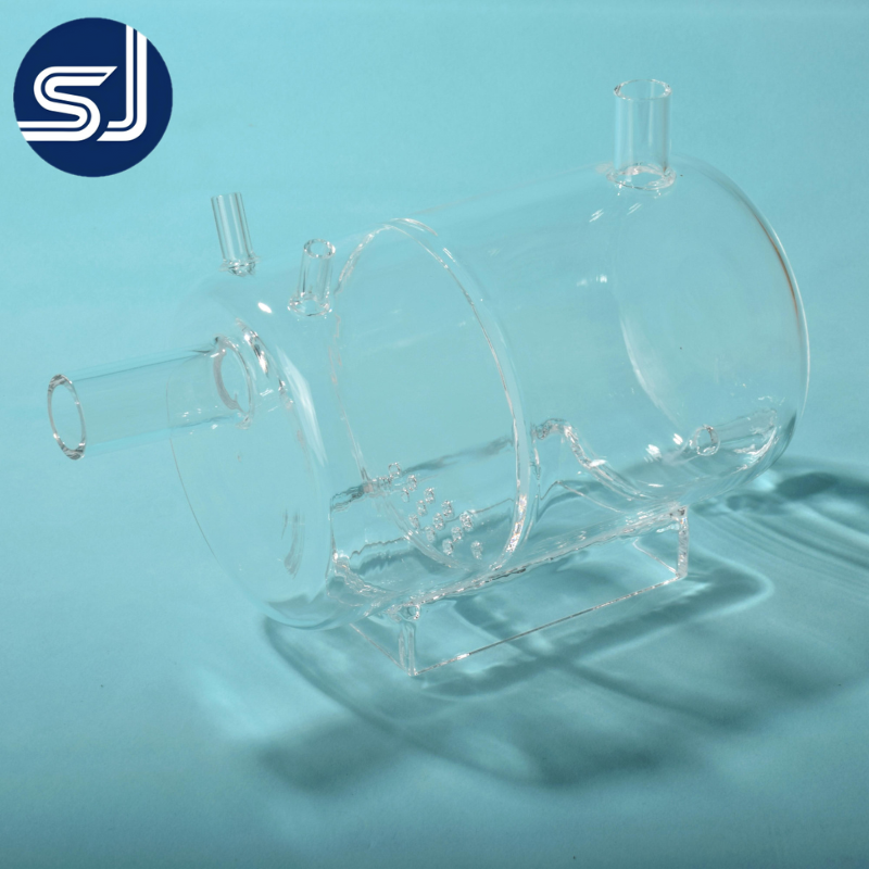
Vulra Quartz applies comprehensive hydrogen-oxygen thermal annealing protocols at 1150°C to completely eliminate residual hoop and longitudinal stresses in bent quartz tubes and welded furnace manifolds, thereby extending structural lifecycle by up to 300% under high-cycle thermal loads.