Precision High-Purity Fused Quartz Lineup
Directly sourced from the crystal capital of Donghai: Certified ultra-low trace-metal fused quartz hardware engineered for chemical vapor deposition (CVD), rapid thermal processing (RTP), and harsh plasma chambers.
Engineering Whitepaper: The Critical Role of Quartz Pedestal Rings in Modern Semiconductor Fabrication
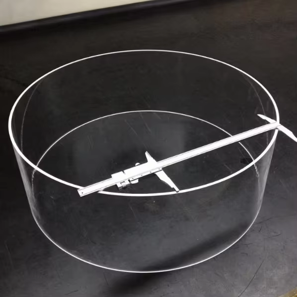
In the ultra-clean vacuum environment of semiconductor processing equipment—spanning plasma-enhanced chemical vapor deposition (PECVD), atomic layer deposition (ALD), low-pressure chemical vapor deposition (LPCVD), and rapid thermal processing (RTP)—the quartz pedestal ring (commonly designated as a wafer susceptor ring, focus ring, edge ring, or pedestal shield) operates as an indispensable thermal, electrical, and chemical barrier. Placed concentrically around the electrostatic chuck (ESC) or ceramic heating pedestal, the quartz pedestal ring directly cradles, aligns, or shields the periphery of 200mm, 300mm, and next-generation 450mm silicon wafers.
Material Chemistry: Why 99.999% Natural Fused Quartz Outperforms in Pedestal Applications
Quartz pedestal rings reside in direct radiative and conductive proximity to temperatures exceeding 1000°C while subject to aggressive halogenated process gases, including Cl₂, NF₃, CF₄, and BCl₃. Under these critical environments, material stoichiometry and trace element purity dictate component lifetime and wafer yield:
1. Alkali & Heavy Metal Exclusion: Trace mobile ionic contaminants (such as Sodium Na⁺, Potassium K⁺, and Lithium Li⁺) act as catastrophic gate dielectric poisons in sub-7nm CMOS and 3D NAND nodes. Our natural high-purity quartz undergoes advanced acid leaching, electro-refining, and vacuum thermal fusion to maintain total alkali levels < 0.8 ppm and heavy transition metals (Fe, Cu, Ni) below detection limits (<0.05 ppm).
2. Hydroxyl (OH⁻) Concentration Control: High hydroxyl concentrations severely reduce the viscosity of fused silica at elevated temperatures, leading to premature structural sagging, geometrical distortion, and cristobalite devitrification above 1050°C. Vulra Quartz utilizes specialized electrical vacuum-fused quartz (OH⁻ < 5–20 ppm) for high-load RTP and furnace rings, raising the softening threshold to 1683°C.
Thermal Shock Mechanics & Birefringence Annealing
Unlike silicon carbide (SiC) or alumina ceramics, fused quartz exhibits an exceptionally low coefficient of thermal expansion (CTE of 5.5 × 10⁻⁷ /°C from 20°C to 1000°C). This allows quartz pedestal rings to survive rapid thermal cycles (ΔT > 120°C/sec) during laser annealing or spike-anneal cycles without thermal fracturing. However, improper machining or localized oxy-hydrogen flame welding introduces latent hoop stresses. Our dedicated annealing cycles (heating to 1180°C with controlled 1.5°C/min ramp-downs) completely dissipate residual stresses, verified via circular polariscope photoelastic analysis with optical retardation ≤ 10 nm/cm.
Technical Specification & Tolerance Matrix: Semiconductor Grade Fused Quartz
| Property / Characteristic | Semiconductor Grade (Standard) | Optical / Ultra-Purity Grade | Verification / Testing Protocol |
|---|---|---|---|
| SiO₂ Purity Level | ≥ 99.99% | ≥ 99.999% (5N) | GDMS / ICP-MS |
| Hydroxyl (OH⁻) Content | ≤ 30 ppm (Dry Grade) | ≤ 5 ppm (Vacuum Fused) | FTIR Spectrometry |
| Continuous Service Temperature | 1100 °C | 1150 °C (Short term 1450 °C) | ASTM C385 Thermal Cycle |
| Coefficient of Thermal Expansion (CTE) | 5.5 × 10⁻⁷ / °C | 5.4 × 10⁻⁷ / °C | Dilatometry (20–1000°C) |
| Total Indicator Reading (TIR Flatness) | ≤ 0.05 mm across Ø300mm | ≤ 0.015 mm custom CNC | Laser Interferometer |
| Surface Roughness (Ra) | Ra 0.4 μm (Precision Ground) | Ra ≤ 0.02 μm (Super-Polished) | White Light Profilometry |
| Bubble & Inclusion Class | DIN 58927 Class 1 | Zero inclusions in critical path | Dark-Field Optical Inspection |
CNC Precision Cold Working vs. Thermal Flame Polishing
Achieving the exacting geometric tolerances demanded by Applied Materials (AMAT), Lam Research, and ASM-type process chambers requires advanced multi-axis CNC machining. Pedestal rings often feature intricate internal vacuum purge channels, step-down counterbores, thermocouple locating notches, and gas distribution micro-holes (Ø ≤ 0.8mm).
While mechanical diamond grinding establishes the exact dimensions, it creates subsurface micro-fractures. Vulra Quartz deploys a proprietary dual-finishing sequence: diamond grinding followed by precision acid etching (HF/HNO₃ controlled bath) to heal microscopic stress risers, followed by automated uniform hydrogen flame-polishing. This eliminates particle-shedding micro-grooves and guarantees a pristine surface that resists radical etching and reduces particle generation inside the wafer chamber.
Why Global Fabs Choose Vulra Quartz
Operating out of No. 9, Dingxin Road in the Jiangsu Donghai Economic Development Zone—the acknowledged crystal capital of China—Lianyungang Vulra Quartz Products Co., Ltd. sits directly atop the world's most concentrated high-purity natural silica sand refining hub.
As an authenticated Custom Manufacturer & Verified Supplier assessed on-site by TÜV Rheinland, we offer drawing-based full customization from a single prototype (MOQ 1 PC) up to recurrent mass-production volume orders for international equipment builders and fab lines.
-
Raw Material Integration: Direct Donghai high-purity quartz reserves ensure uncompromised batch-to-batch chemical homogeneity and non-fluctuating supply.
-
Full-Spectrum Processing: Flame tube drawing, CNC diamond ultrasonic milling, fire polishing, and annealing ovens up to 1250°C under one verified roof.
-
Zero Particle Packaging: Class 1000 cleanroom ultrasonic deionized water wash, double vacuum heat sealing, and suspended shockproof crating.
-
Drawing-Based Feasibility: Pre-production thermal stress analysis and tolerance checks ensure seamless drop-in fit for existing OEM chambers.
Strategic Procurement Outlook: Future Trends in Quartz Pedestal Hardware (2025–2030)
As the global semiconductor industry transitions to gate-all-around (GAA) architectures, sub-2nm lithographic nodes, and ultra-high-aspect-ratio (UHAR) 3D NAND etch processes (>300 layers), the requirements imposed on quartz chamber components are undergoing profound structural shifts:
Procurement Optimization: Total Cost of Ownership (TCO) vs. Purchase Price
Procurement directors in tier-1 fabs are increasingly discarding purchase price per unit as their primary KPI, replacing it with Total Cost of Ownership (TCO). A lower-cost quartz pedestal ring with subtle wall thickness variations, invisible internal bubbles, or inadequate stress annealing causes premature chamber shutdowns, catastrophic in-situ wafer breakage, or micro-particle fallout.
Vulra Quartz supports fab procurement teams by delivering documented certificate of analysis (COA) packages with every shipment, encompassing 100% laser dimensional CMM data, ICP-MS metallic impurity traces, and optical stress birefringence certifications. This eliminates receiving-inspection friction and enables immediate tool installation.
Frequently Asked Engineering & Procurement Questions
Direct answers from our senior quartz application engineers regarding materials, custom tolerances, cleanroom standards, and supply chain logistics.
What is the difference between natural fused quartz and synthetic fused silica for pedestal rings?
What geometric tolerances can your factory guarantee on custom quartz pedestal rings?
What is the minimum order quantity (MOQ) for custom drawing-based quartz parts?
How do you manage thermal stress and prevent in-chamber devitrification?
What export packaging protocols are used to guarantee break-free international transit?
Can you customize ozone-free or synthetic UV-grade quartz components?
How does Vulra Quartz verify product quality before delivery?
What file formats do you accept for engineering drawings and quoting?
Ready to Validate Your Custom Quartz Design?
Consult with our Donghai factory engineers today for comprehensive drawing reviews, material purity evaluations, and instant quote estimates for your semiconductor or laboratory quartz requirements.
Contact Us