Featured Semiconductor Quartzware & Process Components
Explore our drawing-customized fused quartz components serving Daejeon's cleanroom wet benches, furnace tubes, and sample analysis environments. Guaranteed dimensional repeatability and chemical inertness.
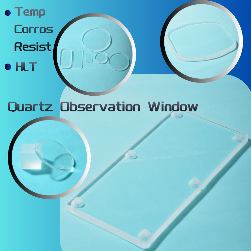
SJ Natural Fused Quartz Polished Plate Optical Clear
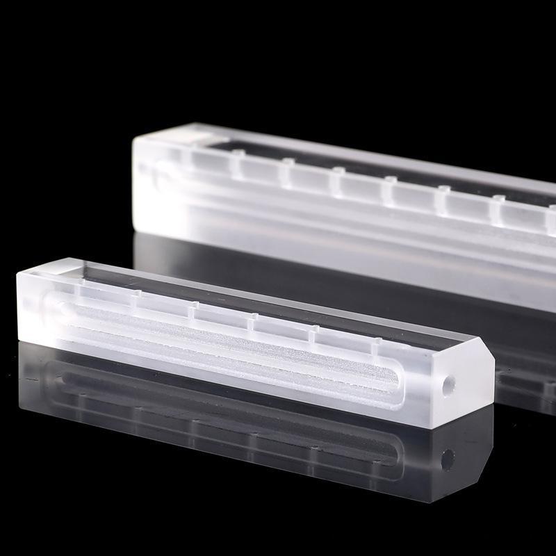
Ultra-Thin Optical Clear Quartz Testing Sheet
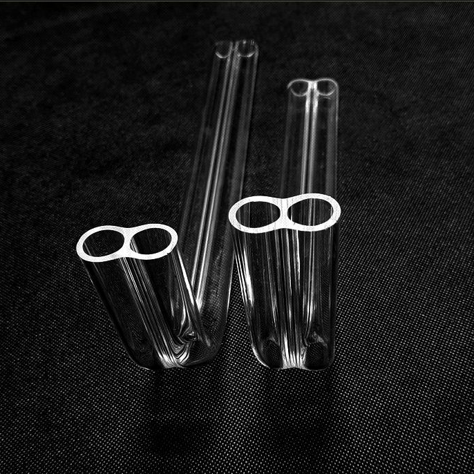
99.999% Purity Quartz Double-Tube Right-Angle Elbow
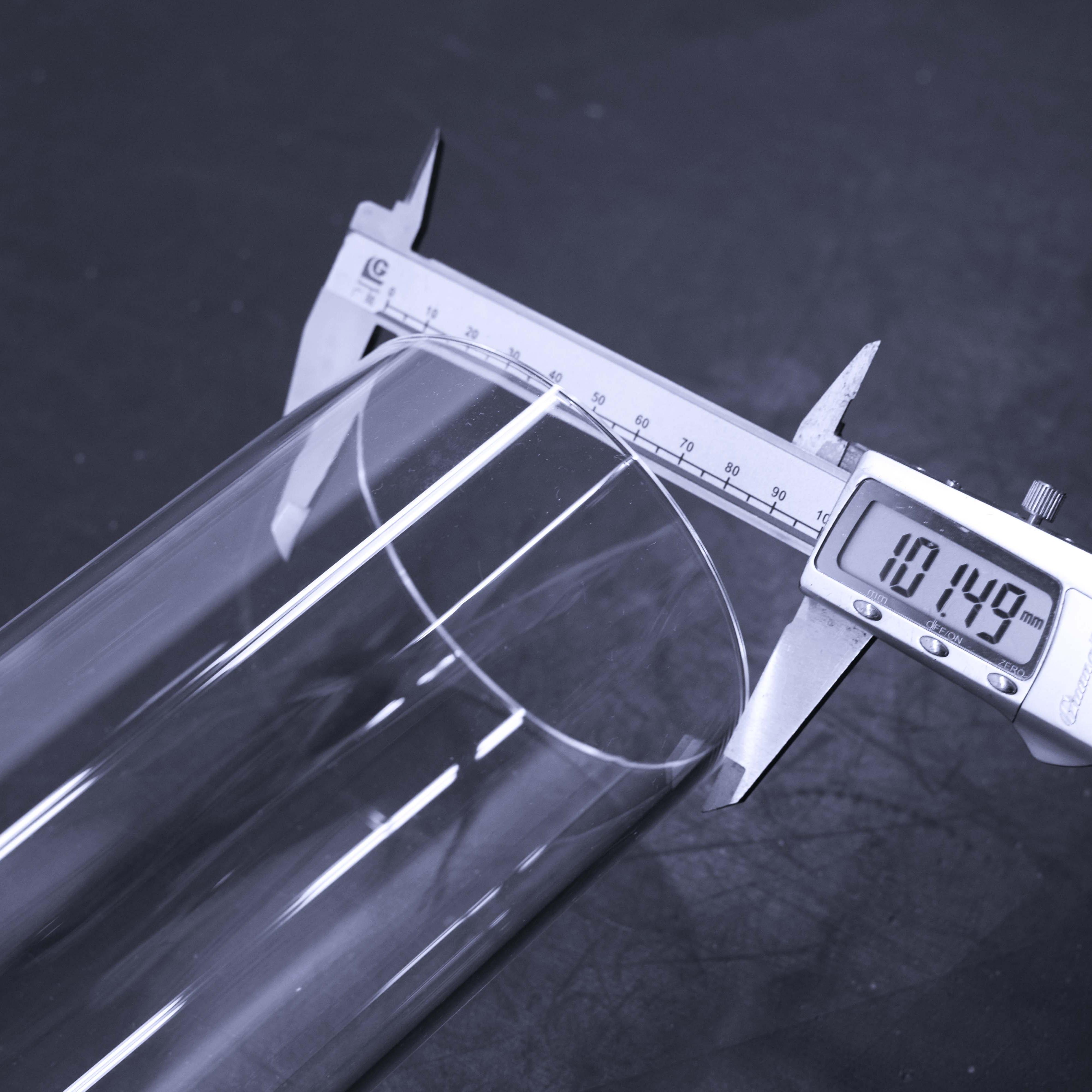
High Purity Transparent Polished Quartz Tube
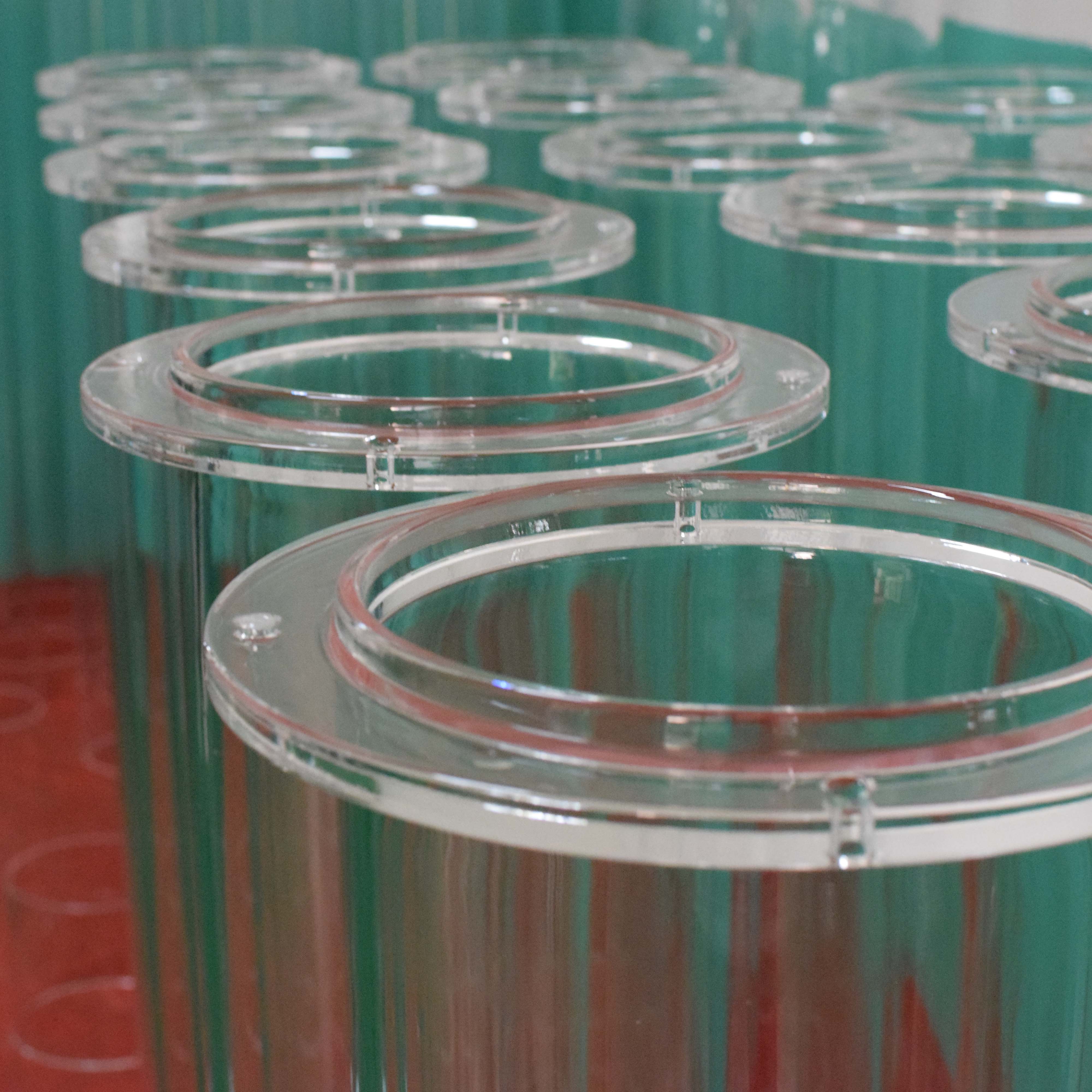
99.999% Single-Crystal Fused Quartz Tube Flange
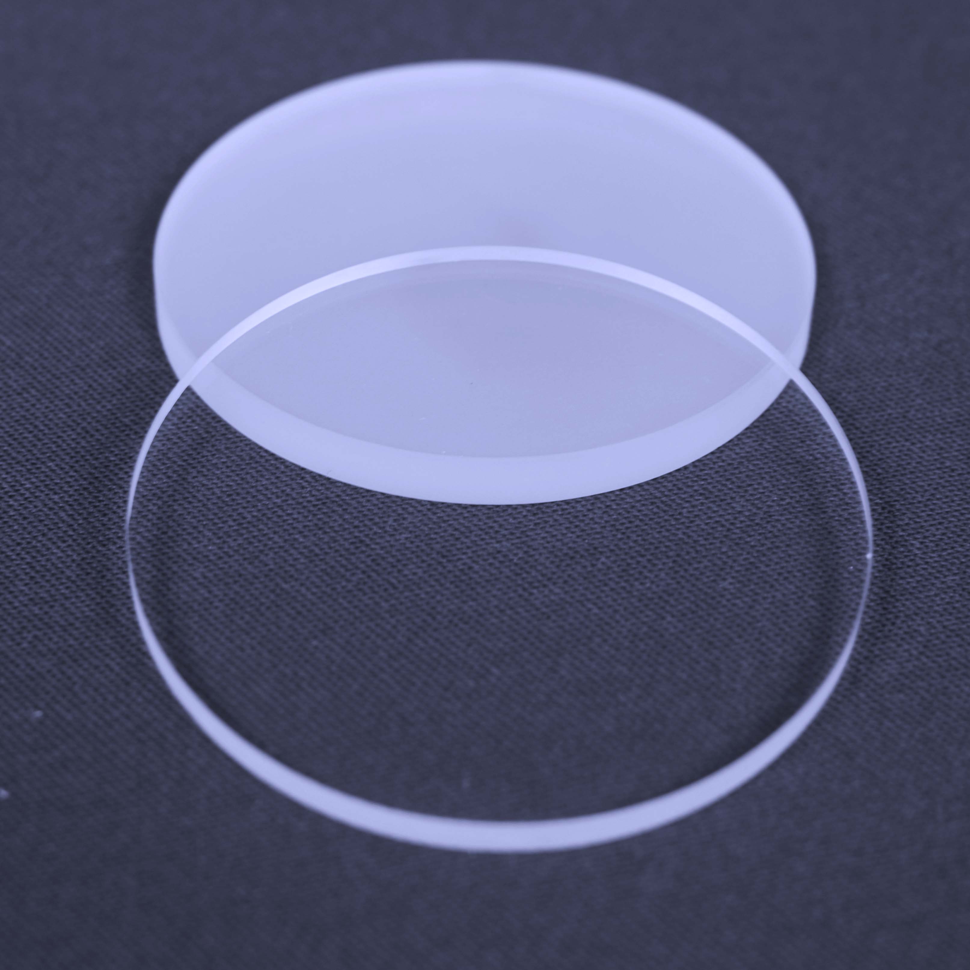
High-Transmittance XRD Quartz Sample Holder
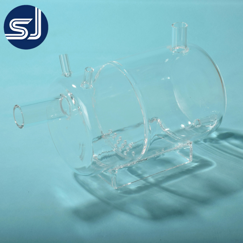
SJ 99.99% Quartz Chemical Flow Splitting Vessel
Hand-Blown Silica Fluid Transfer Vessel & Beaker
High-Precision Quartz Wafer Carriers in the Daejeon Semiconductor Ecosystem
Daejeon Metropolitan City stands as the intellectual engine of South Korea's advanced microelectronics and nanotechnology sectors. Anchored by Daedeok Innopolis, the Korea Advanced Institute of Science and Technology (KAIST), the Electronics and Telecommunications Research Institute (ETRI), and the National NanoFab Center (NNFC), the Daejeon region demands semiconductor process equipment components characterized by unprecedented purity and tight geometric tolerances.
In high-temperature thermal diffusion, oxidation, and Low-Pressure Chemical Vapor Deposition (LPCVD), wafer carriers—commonly referred to as quartz boats or quartz cassettes—serve as the mechanical backbone holding 100mm, 150mm, 200mm, and 300mm silicon and compound semiconductor wafers. With processes routinely scaling past 1050°C and handling corrosive atmospheres containing dichlorosilane, ammonia, and hydrogen chloride, raw material integrity dictates wafer yield.
- Sub-ppb Metal Impurities: Strict alkali metal (Na, K, Li) thresholds preventing gate oxide breakdown in sub-micron device architectures.
- Zero Sagging at 1100°C+: Optimized hydroxyl (OH⁻) content ensuring high annealing stability and creep prevention during extended thermal soak cycles.
- Robotic End-Effector Matching: Precision CNC diamond slotting providing pitch uniformity down to ±0.05mm for automated wafer transfer arms.
Structural Topology & Thermal Kinematics of Quartz Wafer Boats
Understanding why natural fused silica remains the substrate of choice over silicon carbide or alumina ceramics in high-yield semiconductor thermal tooling.
Thermal Shock Resilience
Featuring an ultra-low Coefficient of Thermal Expansion (CTE) of approximately 5.5 × 10⁻⁷ /°C between 20°C and 1000°C, high-purity quartz wafer carriers survive rapid furnace insertion and extraction cycles without structural deformation, micro-fissuring, or thermal stress breakage, protecting delicate multi-thousand-dollar wafer batches.
Precision Slot Geometry
Our 5-axis diamond cold grinding workshops cut custom V-shaped, U-shaped, and contoured slot profiles. Each tooth is fire-polished to eliminate micro-burrs and edge chips, preventing particle shed during high-speed vacuum wafer loading and minimizing the contact surface area to reduce back-side scratch defects.
High-Temperature Creep Resistance
By controlling trace aluminum (Al) dopants and minimizing residual hydroxyl (OH) radicals below 20 ppm in our thermal-grade raw ingots, Vulra quartz carriers retain rigid structural geometry at 1150°C, suppressing the vertical deflection and boat bowing that plagues lower-tier commercial quartzware.
Engineering Material Comparison: High-Purity Quartz Carrier Grades
Selecting the ideal quartz grade for cleanroom applications across Daejeon's R&D fabs and production environments.
| Performance Parameter | Semiconductor High-Temp Grade | Wet-Bench Chemical Grade | Optical Clear Synthetic Grade |
|---|---|---|---|
| Base Purity (SiO₂ %) | ≥ 99.999% (5N) | ≥ 99.99% (4N) | ≥ 99.9999% (6N) |
| Continuous Max Operating Temp | 1150 °C | 1000 °C | 1200 °C |
| Softening Point | 1683 °C | 1660 °C | 1710 °C |
| Trace Fe Content (ppm) | < 0.1 ppm | < 0.5 ppm | < 0.01 ppm |
| Trace Alkali Metals (Na, K, Li) | < 0.4 ppm aggregate | < 1.2 ppm aggregate | < 0.05 ppm aggregate |
| Typical Daejeon Application | LPCVD, Oxidation, Diffusion | Piranha, RCA, HF Etch Cleaning | Deep-UV Litho, Photomask Substrates |
Where Our Quartz Carriers Deploy in Daejeon’s Hi-Tech Corridors
From government-backed nanotechnology institutes to commercial compound semiconductor startups around Yuseong-gu and Daedeok Science Valley.
1. Daedeok R&D Pilot Lines
At institutions like the National NanoFab Center (NNFC) and ETRI, research teams fabricate novel silicon photonics, quantum computing qubits, and sub-5nm CMOS prototypes requiring low-volume, high-mix custom quartz wafer carriers with specialized slot pitches.
2. Compound Semi (GaN & SiC)
Daejeon-based power electronics laboratories conduct ultra-high-temperature epitaxy and annealing on Gallium Nitride and Silicon Carbide wafers. Our heavy-wall fused quartz carriers provide uniform thermal mass and eliminate chemical leaching.
3. Automated Acid Etching
Industrial wet processing stations utilize our quartz cassettes for immersion in boiling sulfuric-peroxide (Piranha) and buffered oxide etchants (BOE), where Teflon boats degrade under temperature or contaminate baths with organic fluoropolymers.
4. Photovoltaic Tandem Cells
Renewable energy labs in Daejeon developing perovskite-silicon tandem cells utilize wide-slot horizontal quartz boats for high-throughput phosphorus oxychloride (POCl₃) liquid diffusion and passivation oxide growth.
Direct From China’s Crystal Capital to Daejeon
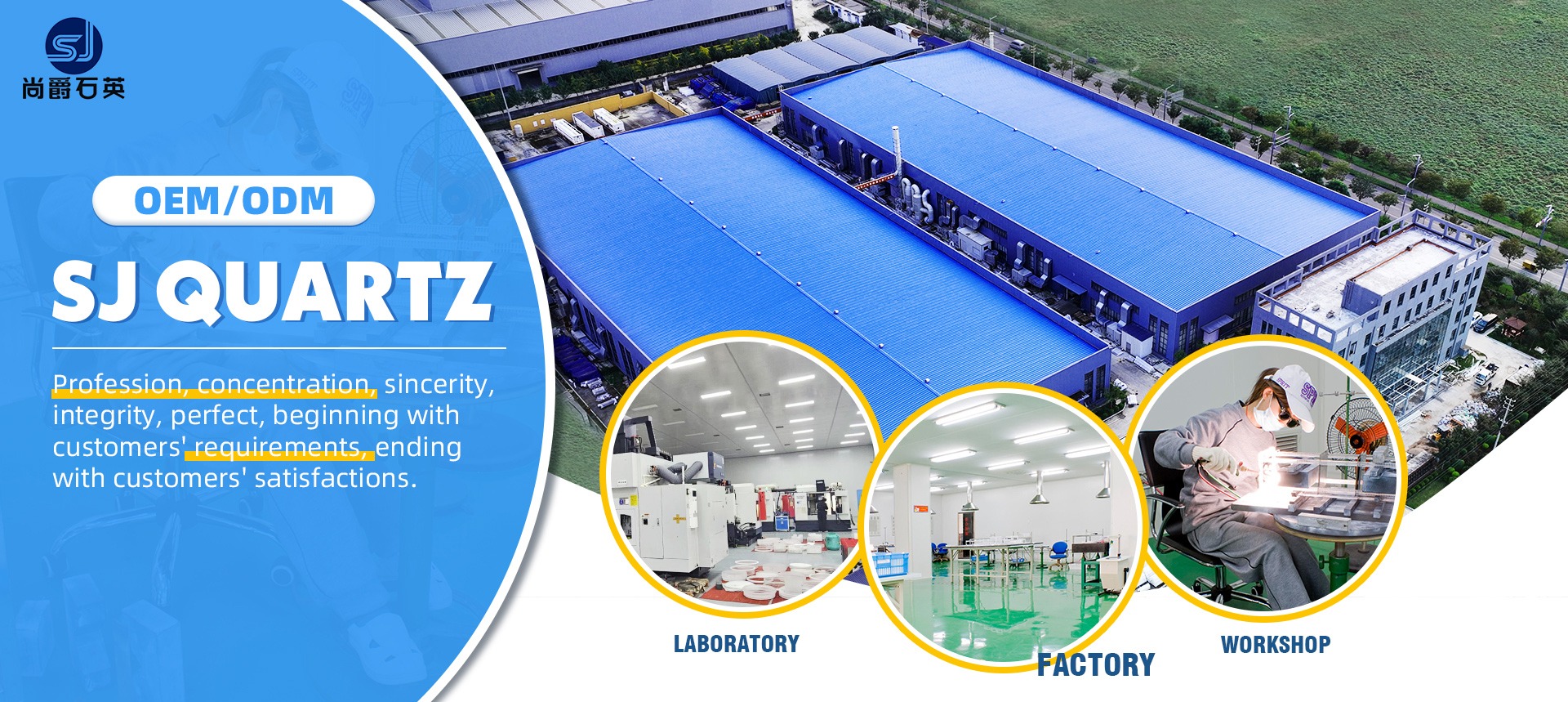
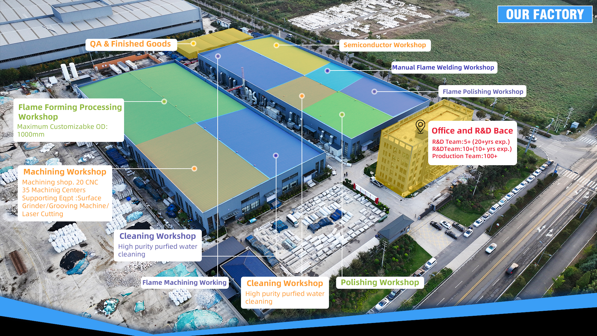
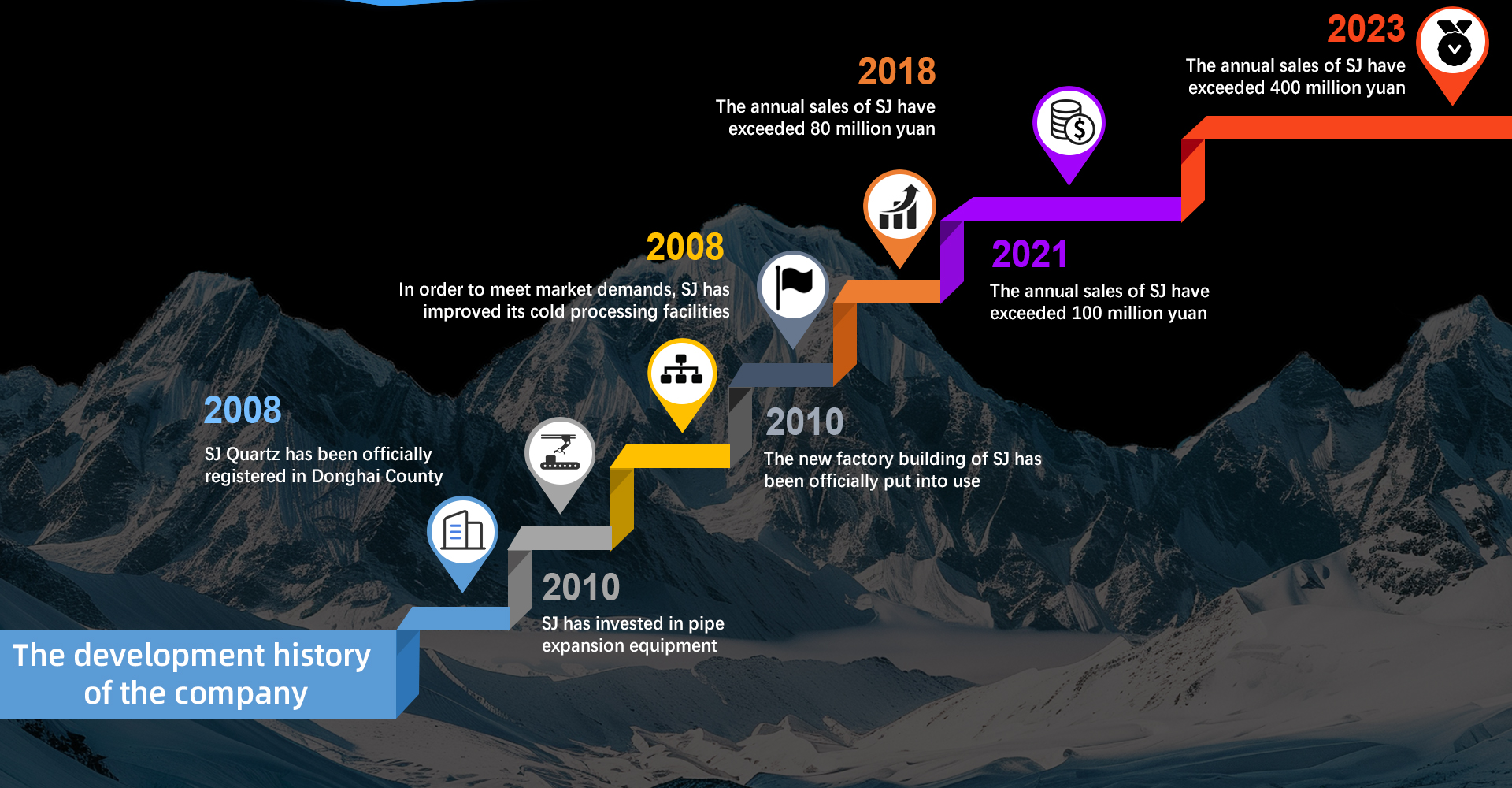
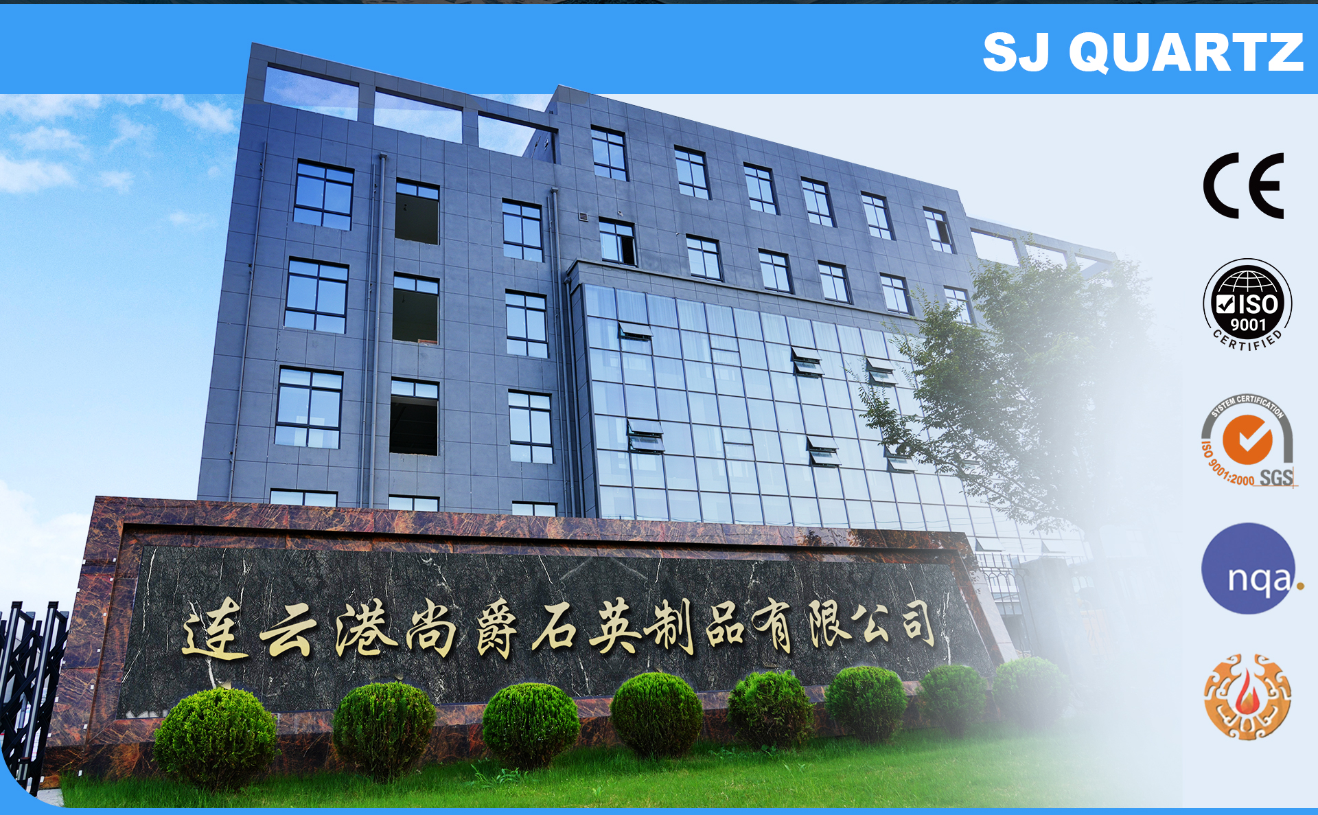
Lianyungang Vulra Quartz Products Co., Ltd. is strategically situated in Donghai County, Jiangsu Province—globally acknowledged as the premier high-purity quartz sand and crystal refinement cluster. Our dedicated manufacturing facility combines raw quartz melting, glassblowing lathes, diamond cold machining, and cleanroom acid leaching in one continuous workflow.


Full-Cycle Workshop Capabilities
High-temperature flame benchforming, micro-slot diamond cutting, and thermal stress relief furnaces configured to meet SEMI standard dimensions.
Evolving Trends in Korea's Semiconductor Quartz Consumables
How Daejeon's transition toward 3D heterogeneous integration and advanced packaging is reshaping wafer carrier procurement requirements.
Shift to Thin-Wafer Handling
As back-side power delivery networks (BSPDN) and 3D stacking require wafers thinned below 50 microns, conventional carrier slots cause wafer bow and micro-cracking. Next-generation quartz boats feature sculpted contoured profiles that cradle the wafer perimeter, distributing gravitational forces uniformly across the contact line.
Low-Particle Plasma Surface Treatments
Cleanrooms in Daedeok Valley are increasingly enforcing sub-10nm particle budgets. Standard chemical cleaning is transitioning toward laser-assisted surface vitrification and plasma etching, removing all surface micro-cavities where contaminants could nucleate during low-temperature ALD runs.
Agile Short-Run Customization
Unlike massive mega-fabs in Pyeongtaek or Yongin running dedicated high-volume recipes, Daejeon's research fab clusters continuously alter substrate dimensions (e.g., small coupons, 4-inch, 6-inch, and 8-inch mixed runs). The market strongly favors agile manufacturers capable of delivering 1-piece bespoke prototypes within 10 to 14 days.
Daejeon Semiconductor Procurement FAQ
Technical, logistical, and commercial answers for purchasing managers, fab engineers, and principal researchers in South Korea.
What CAD file formats do you accept for custom wafer boat fabrication?
Can your quartz carriers match SEMI standard automated end-effectors?
How do you protect fragile quartzware during transit to Daejeon?
What is your minimum order quantity (MOQ) for custom prototypes?
How do your products resist aggressive Buffered Oxide Etch (BOE) solutions?
What material certification and purity analysis do you provide?
What is the standard lead time for delivery to Daejeon?
Can you re-slot or repair cracked quartz boats and furnace tubes?
Accelerate Your Daejeon Fab's Quartz Tooling Procurement
Whether you need a bespoke 25-slot vertical wafer boat for 200mm SiC thermal processing or an ultra-flat optical inspection plate, our engineering team is ready to analyze your technical drawings and provide a competitive quote within 24 hours.