Featured Semiconductor & Lab Quartz Solutions
Manufactured from high-purity natural crystal sand and precision-worked synthetic quartz. Designed to meet the stringent mechanical, thermal, and optical tolerances required across Singapore's advanced high-technology sectors.
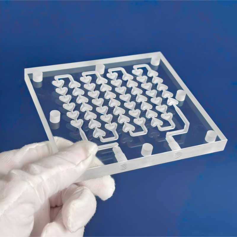
High Thermal Conductance Quartz Interlayer Chips
Circular high-temperature heat-exchange quartz chips with extreme melting point tolerance and uniform thermal dissipation.
View Specifications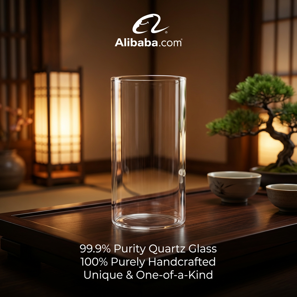
Custom Fire-Polished Pure Silica Reagent Vessels
Clear hand-blown high-purity fused silica cylindrical vessels and quartz tubes engineered for analytical acid digestions.
View Specifications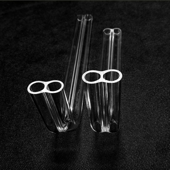
Corrosion-Resistant Quartz Double-Tube Elbows
Right-angle bent double-tube gas injection lines with flame-annealed seams for corrosive semiconductor process gases.
View Specifications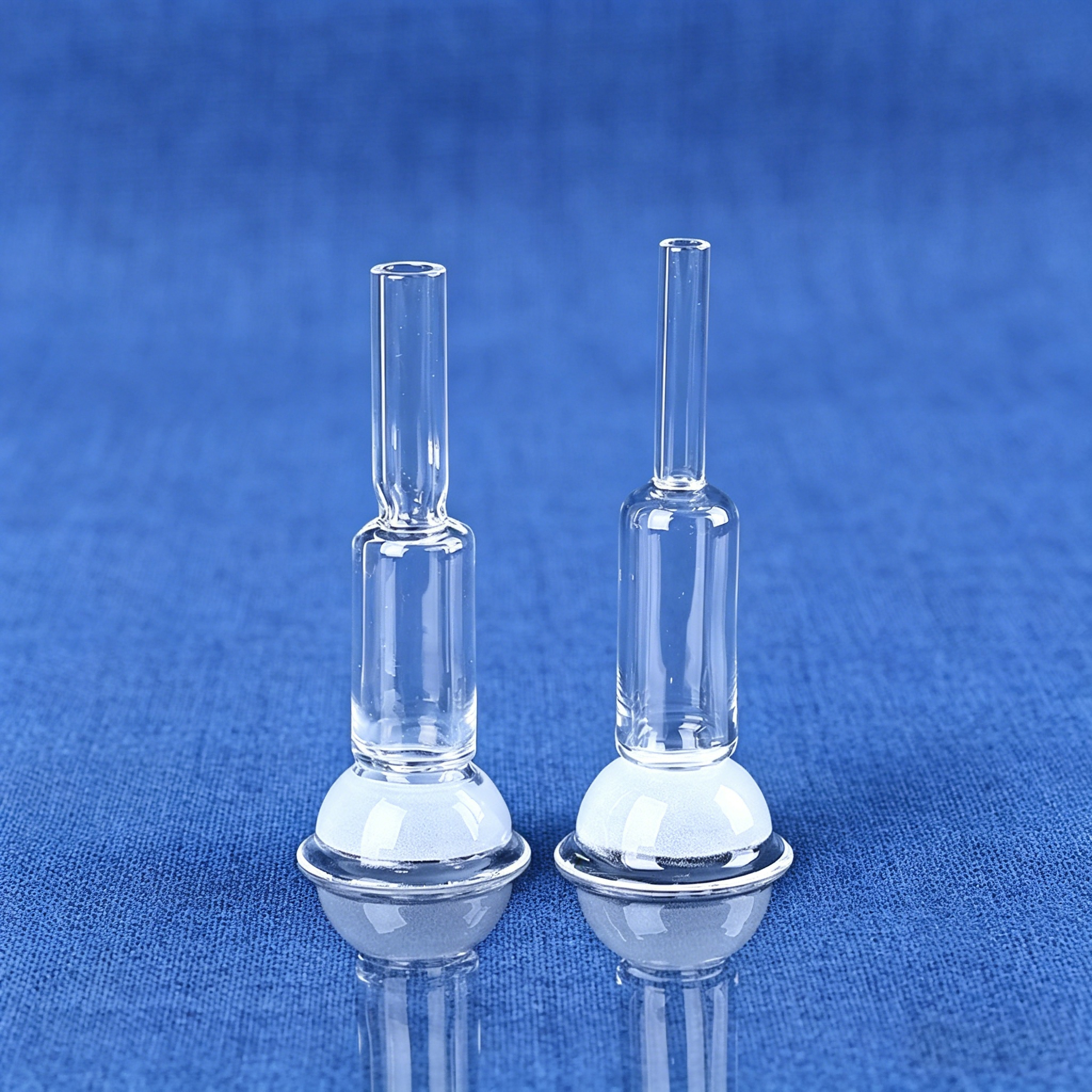
C-Shaped Small-Sized Analytical Quartz BET Tubes
High-precision bending and micro-welding for gas adsorption, surface analysis, and specialized semiconductor vacuum lines.
View Specifications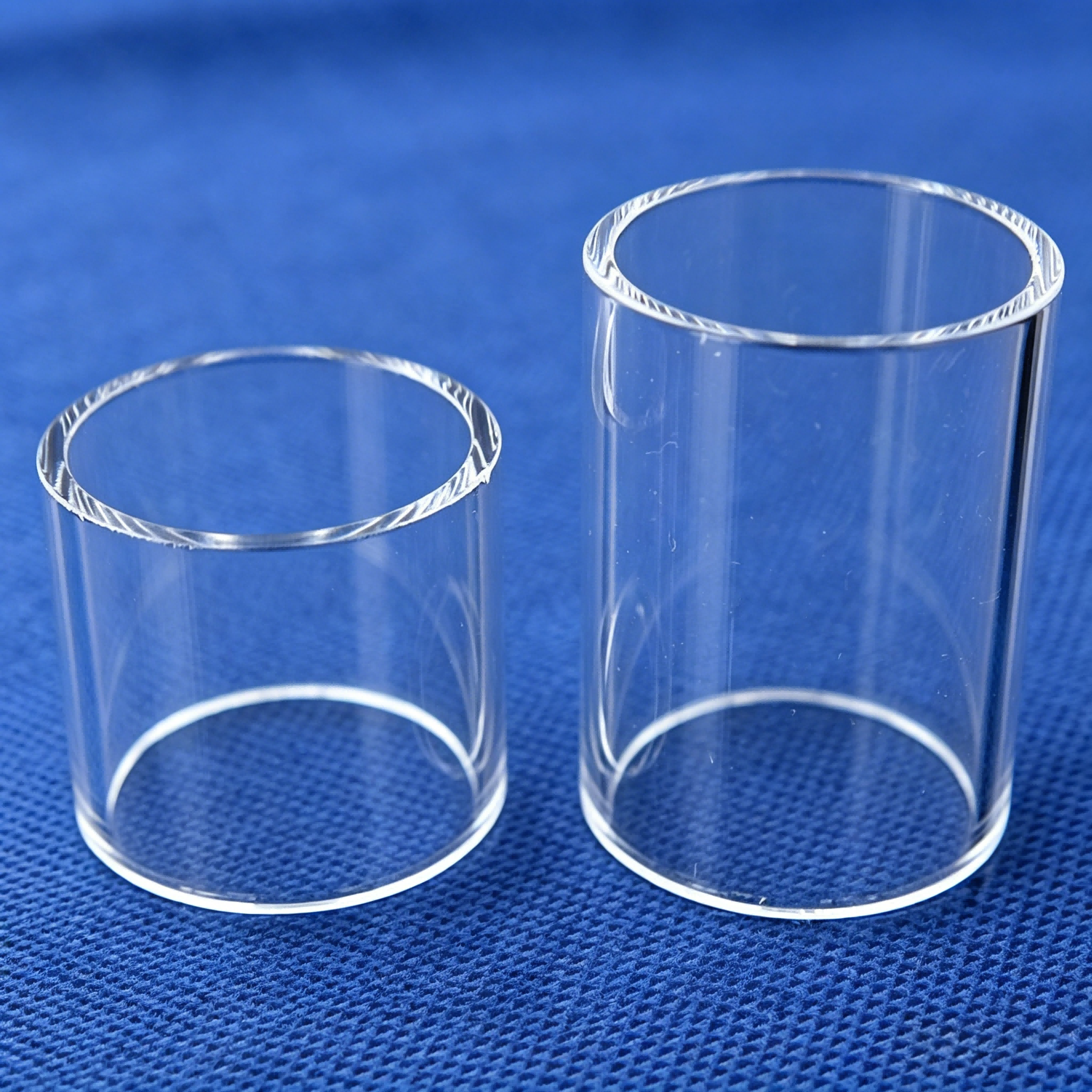
High-Temp Twin-Tube Process Quartz Glass Pipes
Dual-channel structural quartz piping with polished inner/outer surfaces, optimized for inline liquid chemical heating.
View Specifications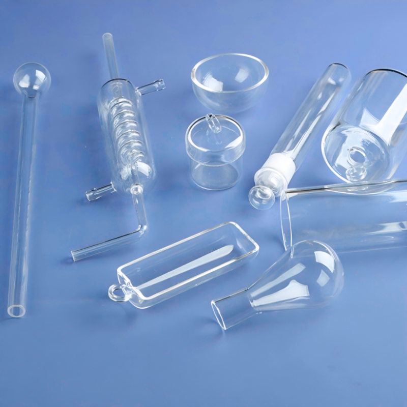
Quartz Furnace Plugging Rods & Test Components
High-frequency thermal barrier rods and tube-end sealing stoppers fabricated from high-density solid fused quartz ingots.
View Specifications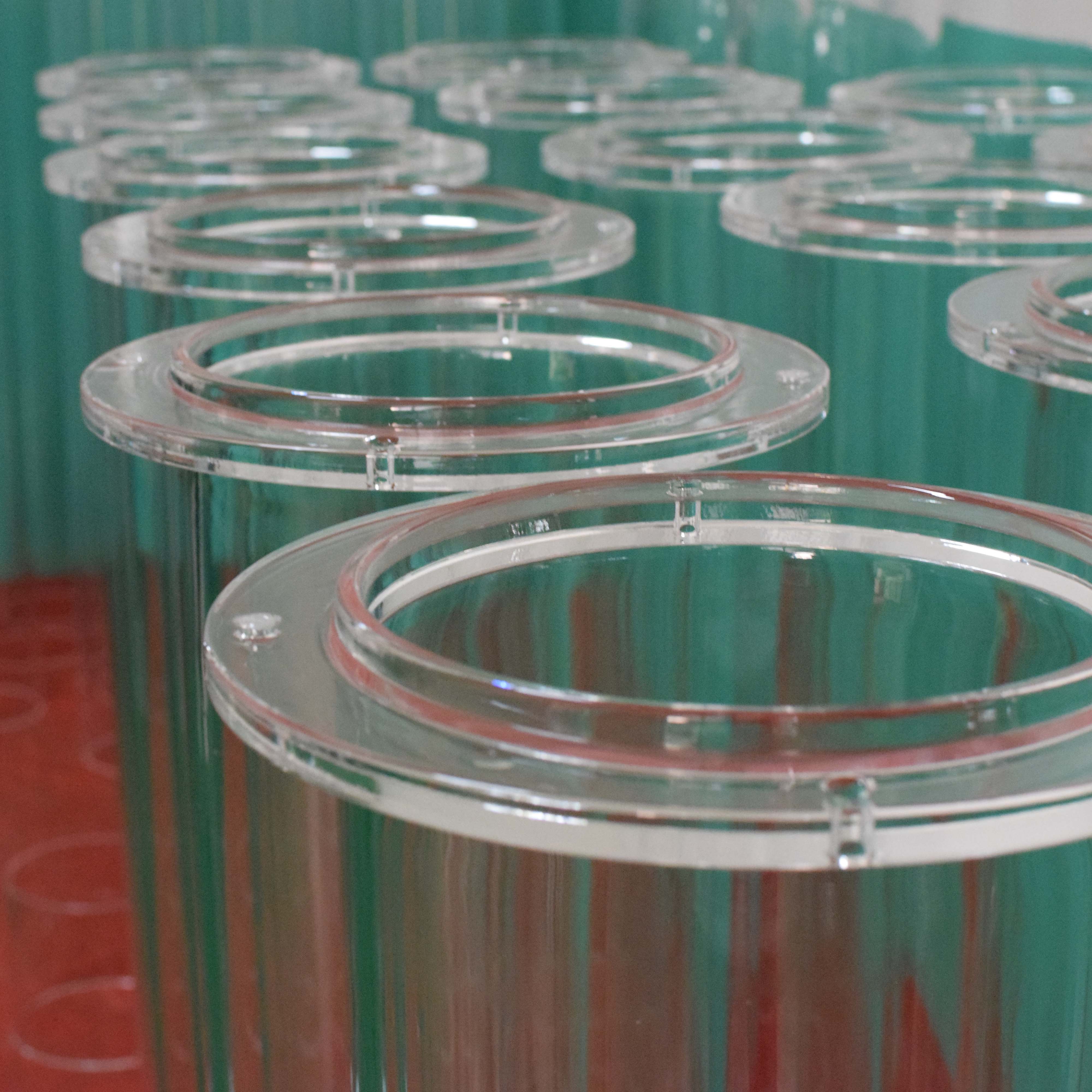
Single-Crystal Grade Flanged Quartz Re-feeder
Seamless ground flanged quartz feed vessels machined to strict concentricity tolerances for wafer fab re-charging systems.
View Specifications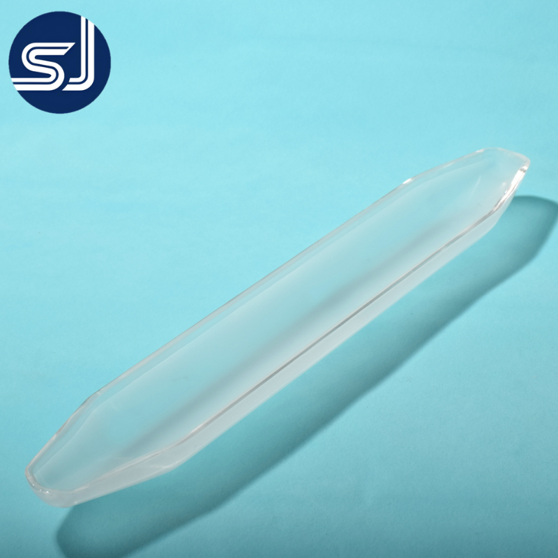
Precision Polished Horizontal Wafer Carrier Boat
Micro-slotted quartz diffusion boats fabricated from pure fused ingot plates, rated for 1100°C continuous tube furnace operation.
View SpecificationsEngineering Fused Quartz Ingots: Metallurgy & Chemical Kinetics
In advanced semiconductor wafer processing and precision optics, the performance of finished diffusion chambers, plasma rings, and lithography windows is strictly dictated by the internal integrity, bubble class, and ionic purity of the primary fused quartz ingot.
1. Primary Fusion Methodologies: Electric Arc vs. Oxy-Hydrogen Flame Fusion
Fused quartz ingots (vitreous silica) represent the solid-state cornerstone of thermal wafer processing. At Lianyungang Vulra Quartz Products Co., Ltd., raw high-purity natural silica sand from Donghai is refined through multi-stage beneficiation, acid de-ironing, and flotation to achieve SiO₂ purity levels of 99.99% to 99.999% (4N to 5N). The conversion of this crystalline quartz into an amorphous vitreous ingot is achieved via two primary thermal routes:
Two-Step Vacuum Induction Fusion (Electric Arc): Granular quartz is melted under deep vacuum within tungsten-mesh or graphite-lined resistance furnaces exceeding 2000°C. This methodology yields high-density cylindrical ingots characterized by ultra-low hydroxyl (OH⁻) content (<5 ppm to <20 ppm). Such low-OH structural ingots prevent optical bubbling, micro-expansion, and thermal sagging during sustained thermal cycles in 300mm diffusion processes.
Flame Fusion (Verneuil Method): High-purity silica feed sand is introduced through a specialized oxy-hydrogen torch, consolidating drop-by-drop onto a rotating pedestal. This process eliminates refractory contact contamination, creating ingots with exceptional visual clarity and minimal heavy metal trace elements, ideal for optical windows, plasma etching rings, and chemical vapor deposition (CVD) bell jars.
Thermal Shock Resistance
Due to an exceptionally low coefficient of thermal expansion (CTE of 5.5 × 10⁻⁷ /°C from 20°C to 1000°C), our fused quartz ingots can withstand rapid temperature differentials exceeding 1000°C without micro-fracturing or structural failure, enabling zero-fatigue fast thermal ramp cycles.
Devitrification Resistance
Under continuous temperatures above 1150°C, ordinary quartz undergoes surface phase transformation into cristobalite. Vulra's strict control over alkali metals (Na, K, Li < 0.5 ppm total) inhibits nucleation kinetics, extending component operating life in aggressive Singapore wafer foundries.
Optical Transmittance
From 260 nm in the deep ultraviolet up into the near-infrared spectrum (2500 nm), our optical ingot grades provide transmission rates exceeding 90%. Precision core selection and vacuum degasification ensure low striae, zero inclusions, and isotropic refractive index homogeneity.
Material Performance & Impurity Profile Matrix
Comparing elemental specifications, physical parameters, and application thresholds across standard and specialty fused quartz ingot grades supplied to the Singapore industrial corridor.
| Physical / Chemical Property | Semiconductor Grade (VQ-Semi) | Optical Clear Grade (VQ-Optic) | Ozone-Free Doped (VQ-OFR) | High-Temperature Low-OH (VQ-IR) |
|---|---|---|---|---|
| SiO₂ Purity Level | ≥ 99.999% (5N) | ≥ 99.995% | ≥ 99.99% | ≥ 99.999% |
| Total Alkali Content (Na, K, Li) | < 0.4 ppm | < 1.0 ppm | < 1.5 ppm | < 0.3 ppm |
| Hydroxyl Content (OH⁻) | < 30 ppm | 150 – 200 ppm | < 30 ppm | < 5 ppm |
| Softening Point (log η = 7.6) | 1683 °C | 1665 °C | 1650 °C | 1710 °C |
| Annealing Point (log η = 13.0) | 1215 °C | 1180 °C | 1170 °C | 1240 °C |
| Dielectric Constant (1 MHz) | 3.75 | 3.80 | 3.82 | 3.70 |
| Typical Processing Application | LPCVD, Dry Oxidation, Diffusion | Spectroscopy, Laser Windows, Prisms | Ozone-Free UV Curing, Photolysis | Epitaxy, Sputtering Targets, Crucibles |
Localized Application Scenarios in Singapore City
Singapore stands as an essential pillar in global semiconductor manufacturing, representing over 11% of global semiconductor market share and roughly 20% of global semiconductor manufacturing equipment output. Our fused quartz ingots directly empower precision toolmakers and fab lines across the island.
Wafer Fab Parks: Tampines, Pasir Ris & Woodlands
Within Singapore's primary fab corridors hosting world-scale foundry complexes (SSMC, UMC Fab 12i, GlobalFoundries Singapore, Vanguard-TSMC JVC), quartzware precision is directly coupled to wafer yields. Fused quartz ingots are sliced, hollowed, and machined into large-bore diffusion furnace tubes, quartz lift pins, wafer transfer paddles, and etching quartz containment rings that endure aggressive fluorine (CF₄/CHF₃) and chlorine plasma environments with minimal particulate spalling.
Jurong Innovation District & A*STAR Research
Singapore's focus on deep-tech innovation at one-north, NUS, NTU, and A*STAR research institutes (IME, IMRE) requires bespoke micro-fluidic substrates, custom-dimensioned fused silica reactor crucibles, and optical waveguides. Our capacity to machine custom quartz components directly from monolithic ingots allows research teams to evaluate novel compound semiconductor alloys (GaN-on-Si, SiC) at prototype scale from a single piece.
Optical Transceivers & Green Data Infrastructure
With Singapore solidifying its position as Southeast Asia's primary cloud and AI data center hub, optical interconnect fabrication is accelerating. Low-bubble optical quartz ingots serve as substrates for collimator arrays, micro-lens preforms, and high-frequency dielectric insulators that reduce optical transmission losses in high-density multi-terabit co-packaged optic architectures.
Singapore Market Trends & Supply Chain Evolution
Navigating the intersection of Singapore's RIE2025 (Research, Innovation and Enterprise 2025) Plan, wafer manufacturing capacity expansions, and resilient factory-direct procurement paradigms.
1. Nearshore Factory-Direct Partnerships vs. Intermediaries
Singaporean procurement directors across Tuas, Jurong, and Changi North are increasingly shifting away from multi-tiered third-party distributors who impose 16 to 24-week delivery lead times and high inventory markups. By establishing direct OEM/ODM supply lines with our manufacturing facility in Donghai, Singaporean fabs achieve:
- Rapid Technical Turnaround: Engineering review of 2D/3D CAD drawings within 24 hours.
- Short Transit Windows: Rapid 3 to 5-day air-freight door-to-door cycles via Changi Airfreight Centre or 7-day consolidated container freight via PSA Singapore terminals.
- Cost Optimization: Transparent Tier-1 factory pricing without margin compounding by local agents.
2. Stringent Class 100 Cleanroom Packaging Requirements
Singapore's high-density wafer fabrication leaves zero margin for sub-micron particulate contamination. Ordinary export packaging fails fab receiving audits. Vulra implements an end-to-end clean handling workflow specifically compliant with Singapore semiconductor standards:
- Acid Etch & Ultrasonic Leaching: Submersion in multi-stage HF/HNO₃ acid baths to strip residual surface contaminants.
- 18.2 MΩ·cm DI Water Rinsing: Cleanroom-grade cascade washing eliminating metallic ionic residues.
- Dual-Layer Clean Vacuum Bagging: Nitrogen-purged, antistatic inner heat-sealed packaging, ready for direct transfer into Singapore cleanroom gowning airlocks.
Integrated Donghai Manufacturing Infrastructure
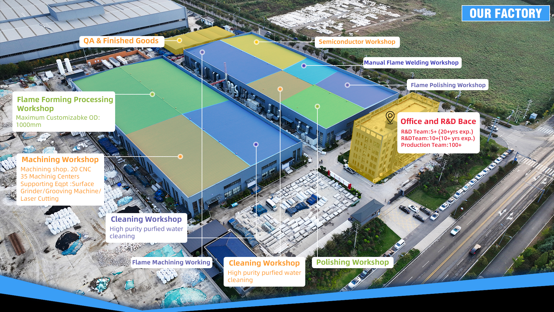
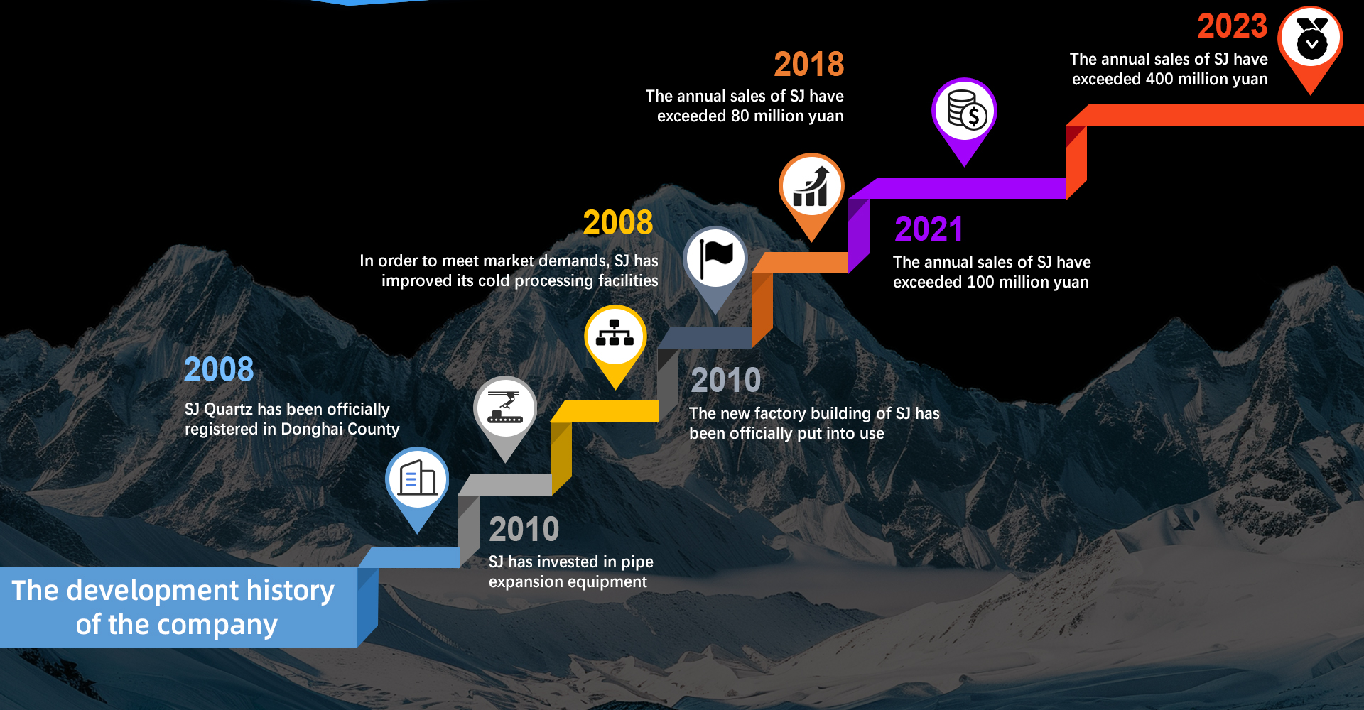
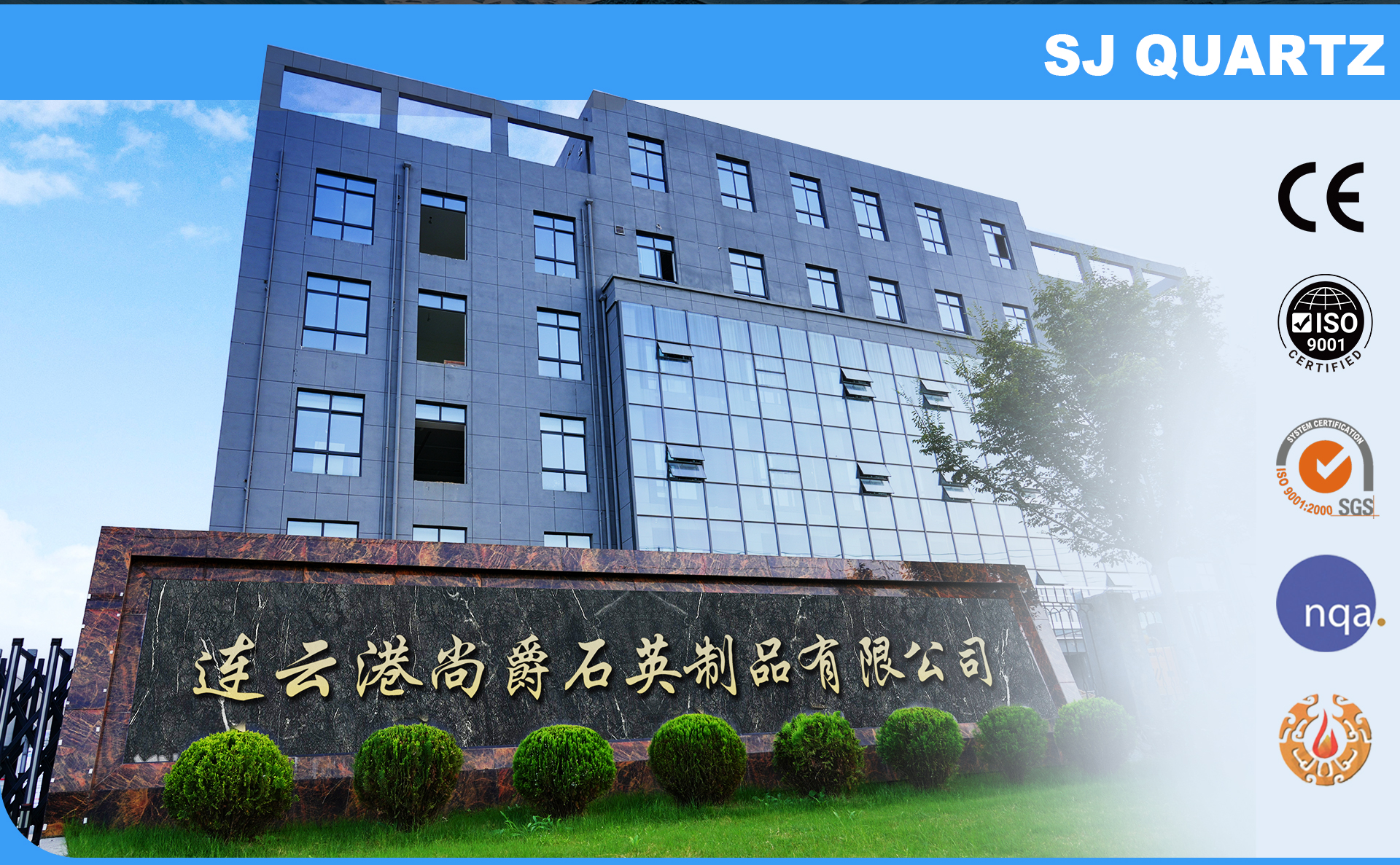
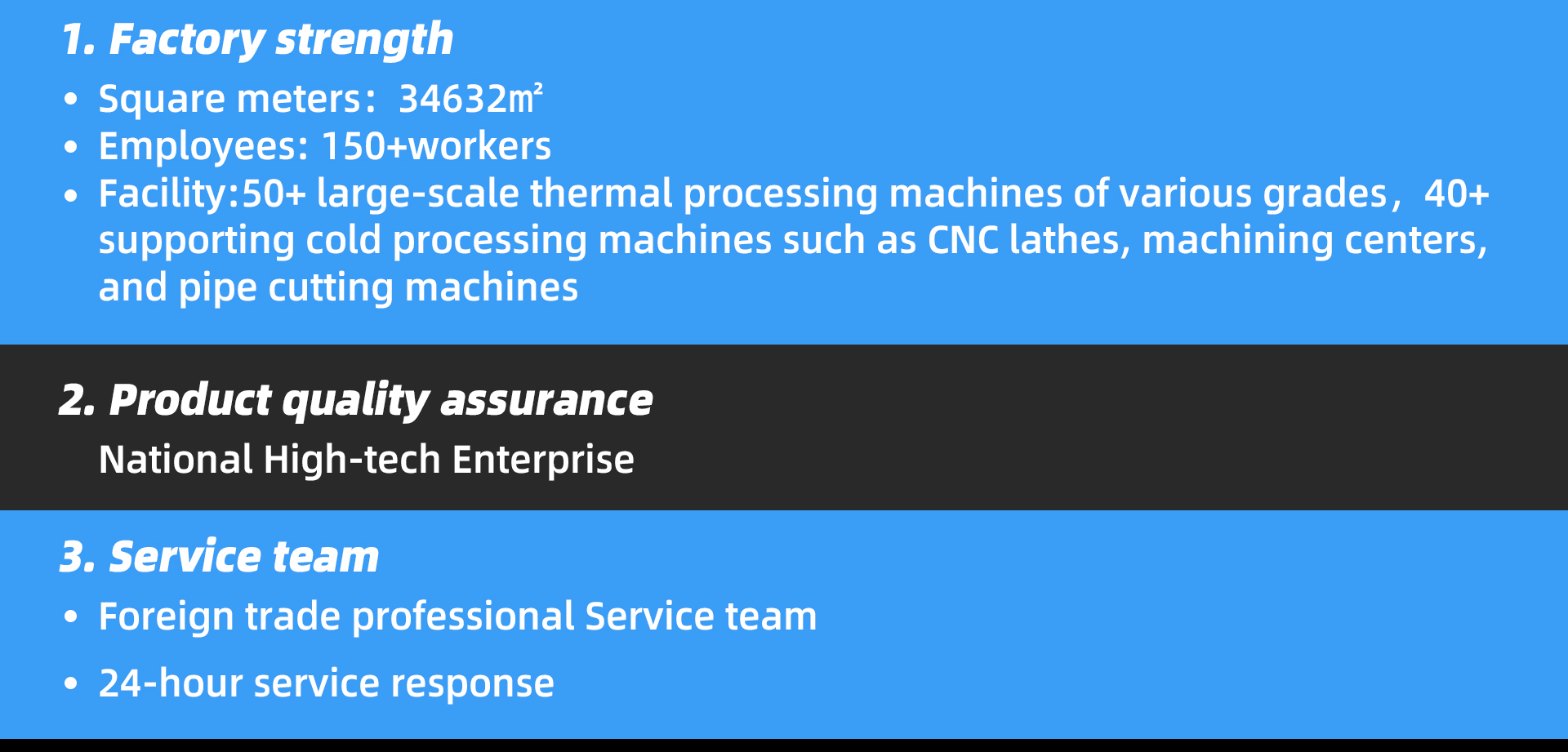
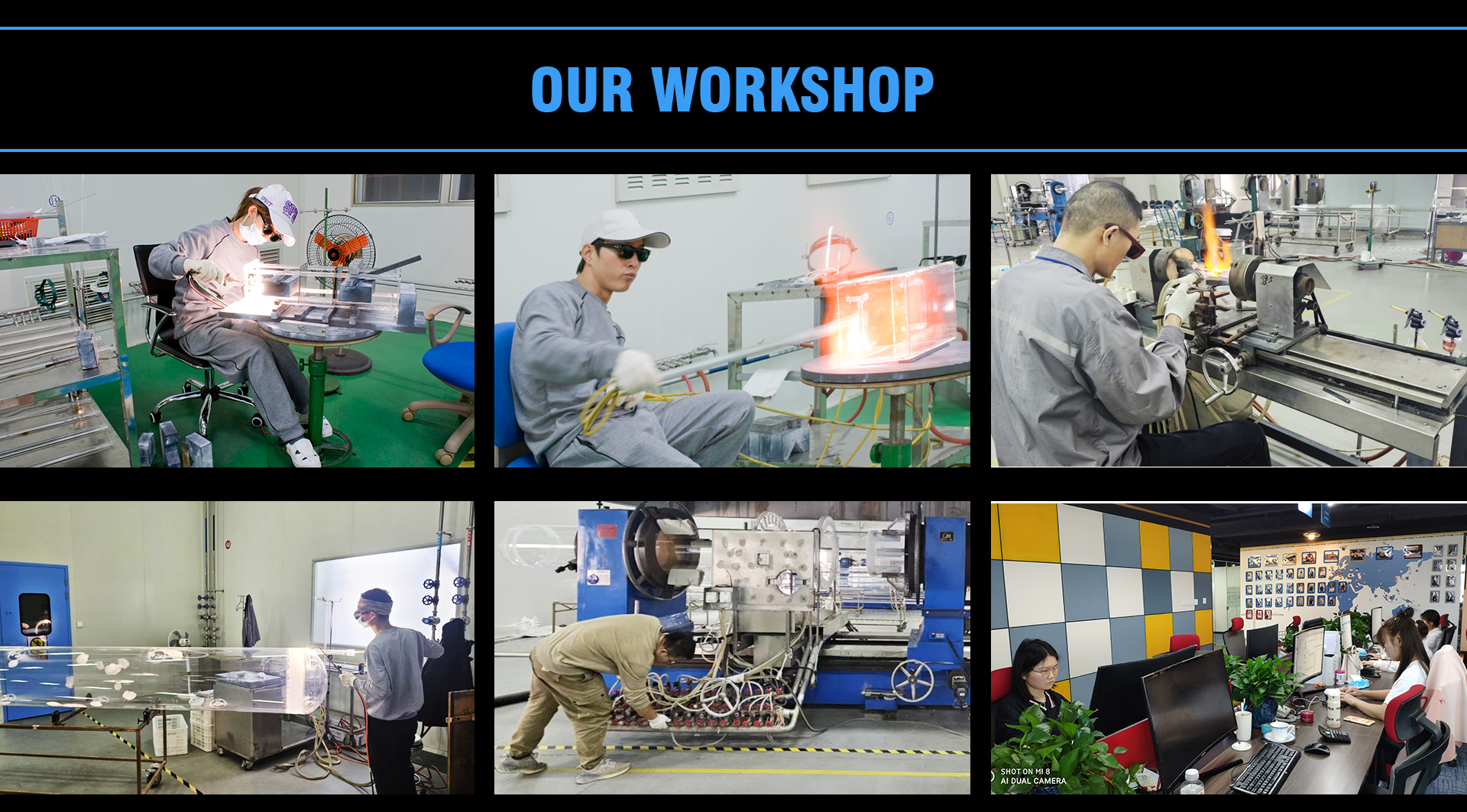
Headquartered at No. 9, Dingxin Road, Jiangsu Donghai Economic Development Zone—the world-renowned crystal capital—Lianyungang Vulra Quartz Products Co., Ltd. combines sovereign raw crystal resources with high-precision fabrication.
Oxy-Hydrogen Flame Working
Hot-forming lathes for tube welding, necking & flanging
Diamond CNC Cold Machining
Chip-free ultrasonic slotting, core drilling & slicing
Lapping & Optical Polishing
Surface roughness down to Ra < 0.2 nm for laser viewports
Controlled Stress Annealing
Computerized thermal ramps eliminating mechanical internal strain
Ultra-Pure Acid Leaching
Decontamination and double vacuum packaging for fab entry
CMM & Spectrophotometry QC
100% dimensional, bubble & optical transmission verification
TÜV Rheinland
On-site assessed manufacturing premises, legal registration, and capacity authenticated.
CE Compliance
Conformity with European Union health, safety, and environmental protection directives.
RoHS Verified
Fully compliant with hazardous substance restriction for lead, cadmium, and hexavalent chromium.
Drawing-to-Part
Full CAD/CAM engineering review for wall thickness, joint stress, and thermal load factors.
Singapore Fused Quartz Procurement FAQ
Common inquiries addressed by our senior application engineering team to support supply chain, quality assurance, and fab equipment engineers in Singapore.