Featured Semiconductor Grade Quartz Components
Precision-manufactured from high-purity natural silica sand and synthetic quartz precursors. Configured to exact customer CAD drawings with full traceability for Bern's high-tech manufacturing base.
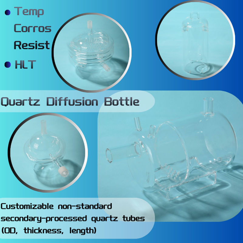
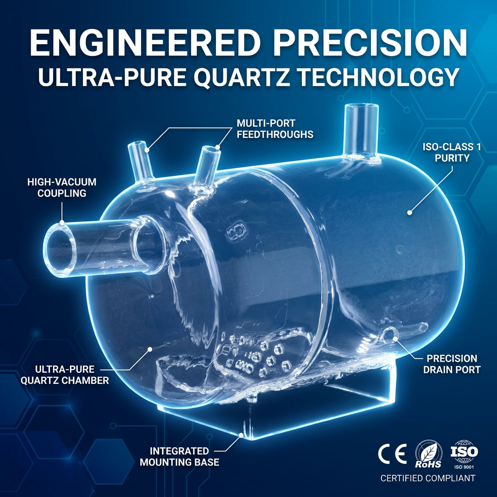
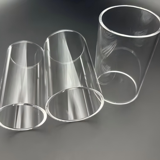
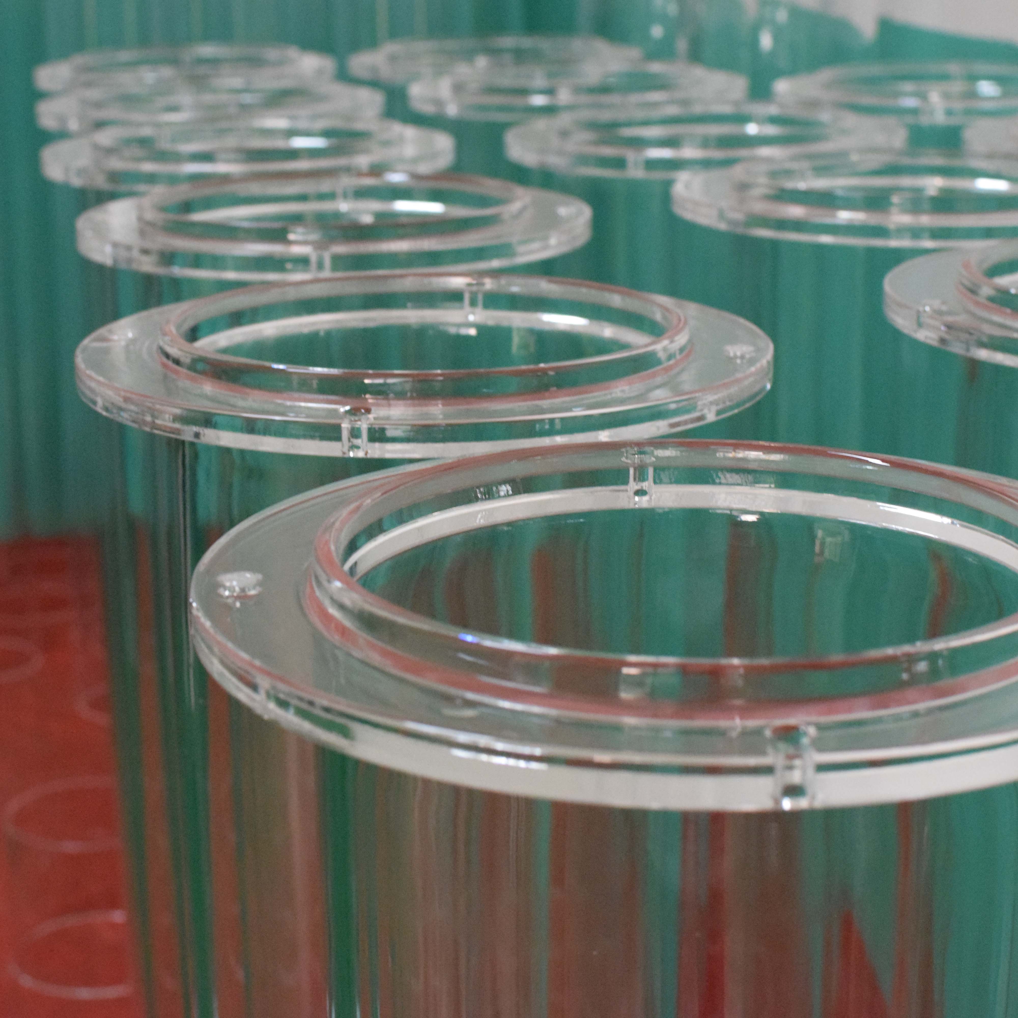
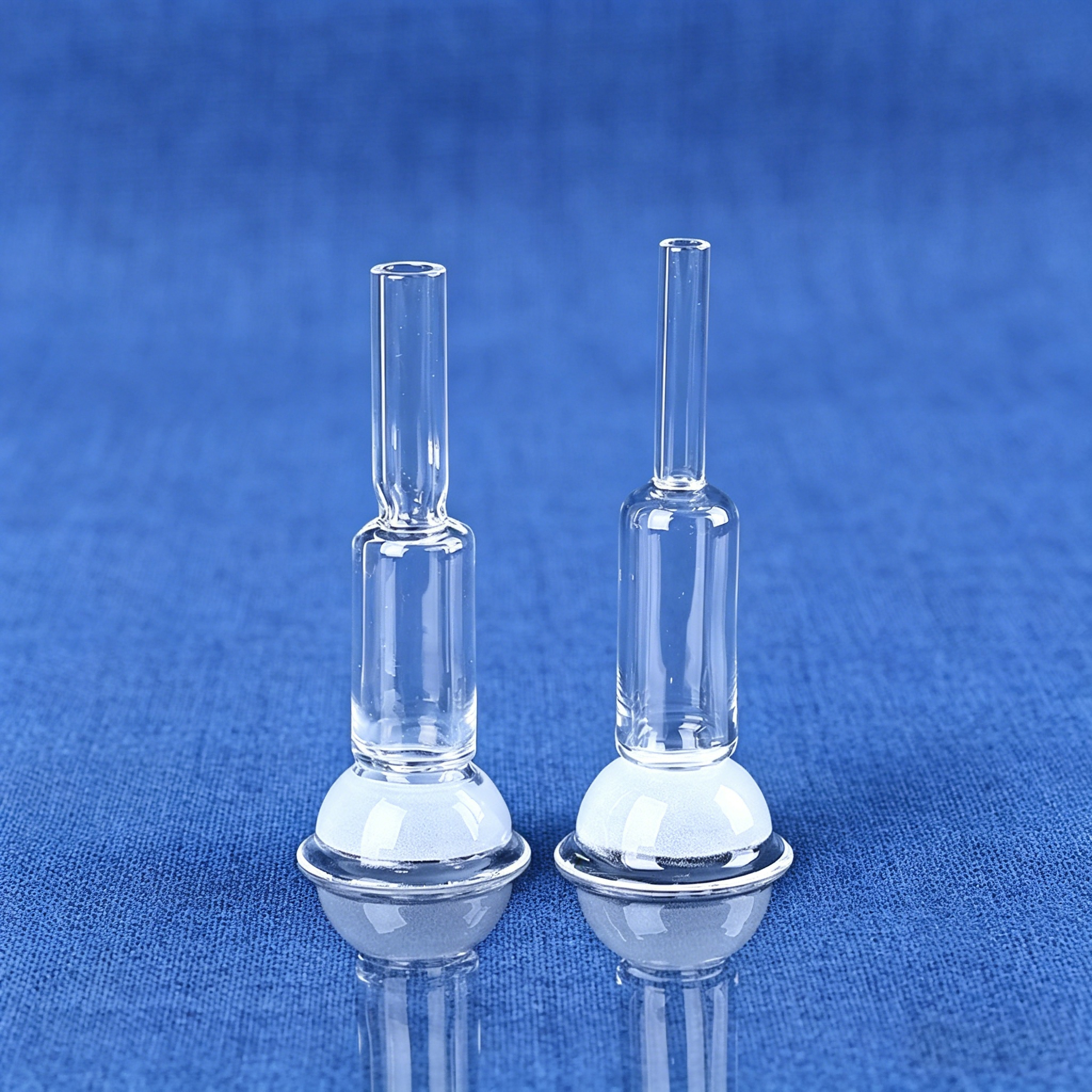
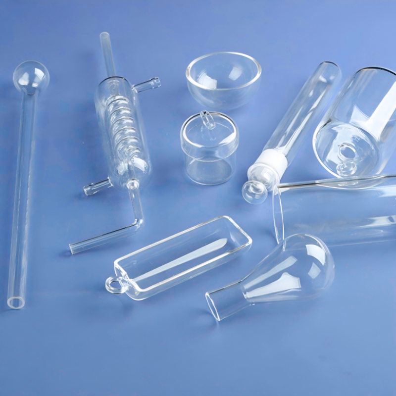
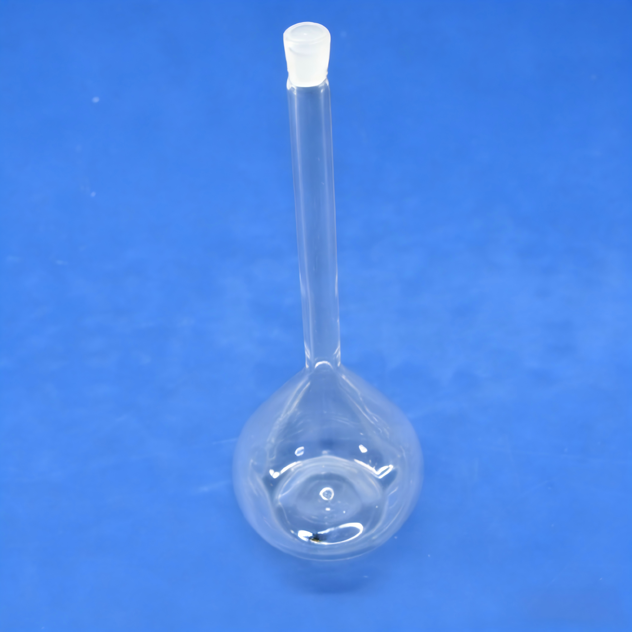
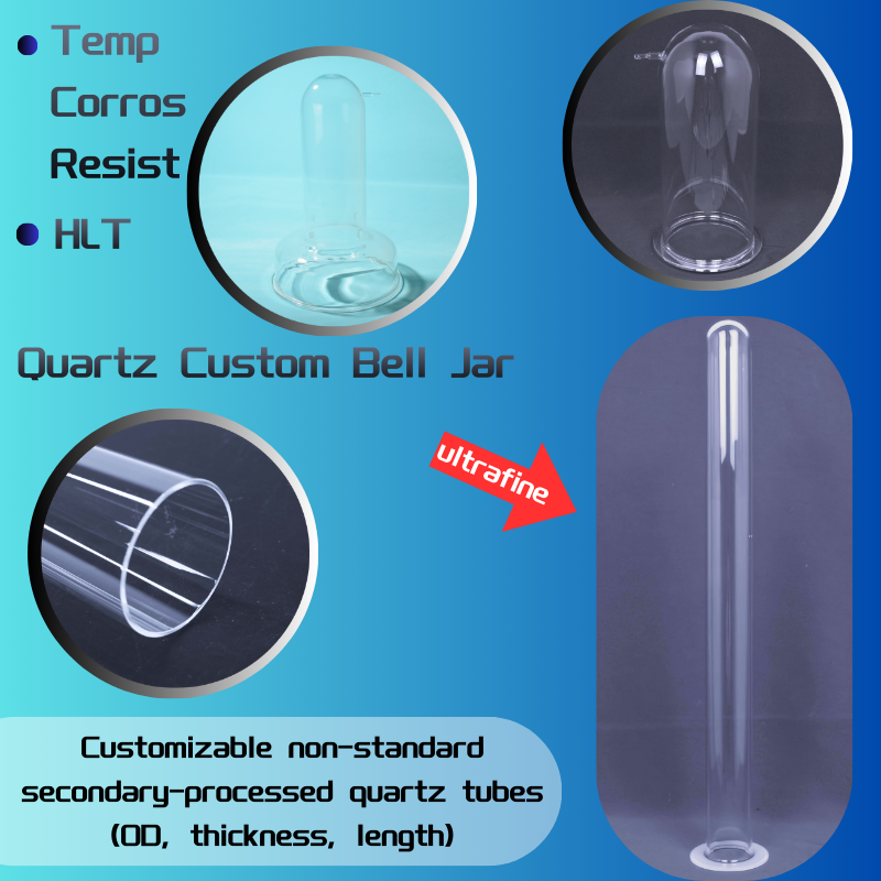
Semiconductor Grade Fused Quartz Engineering for the Bern Innovation Hub
An authoritative metallurgical and structural evaluation of high-purity fused silica (SiO₂) components, thermal stress dynamics, and precision fabrication requirements for Swiss OEM system integrators.
In high-tech precision manufacturing, the Canton of Bern and the surrounding Swiss Espace Mittelland represent one of the world's most concentrated clusters for microtechnology, advanced photonics, medical instrumentation, and semiconductor research. Facilities collaborating with research entities such as the University of Bern (Institute of Applied Physics), CSEM, and precision engineering centers demand ultra-pure, dimensionally invariant materials capable of withstanding extreme thermal gradients, aggressive halogen plasma environments, and ultra-high vacuum conditions. Semiconductor grade quartz glass represents the structural and process backbone of these advanced systems.
Material Metallurgy: Natural Fused Quartz vs. Synthetic Fused Silica
Understanding the distinction between natural electric-fused quartz and synthetic chemical-vapor-deposited (CVD) fused silica is fundamental to optimizing operational cost without sacrificing performance. Natural fused quartz is manufactured by melting high-purity natural silica sand sourced from premier crystal reserves (such as Donghai, China). It exhibits exceptional high-temperature mechanical stability, an extraordinarily low coefficient of thermal expansion ($5.5 \times 10^{-7}/\text{K}$), and high viscosity at elevated temperatures, rendering it the optimal choice for thermal diffusion tubes, furnace boats, wafer carriers, and process chambers operating above 1000°C.
Conversely, synthetic fused silica is synthesized via the vapor-phase oxidation of silicon tetrachloride ($\text{SiCl}_4$) or organic silanes. This process yields a material virtually free of metallic impurities (transition metals $< 0.1\,\text{ppm}$), offering superior optical transmission deep into the vacuum-ultraviolet (VUV) spectrum ($160\,\text{nm} - 260\,\text{nm}$). While synthetic silica excels in lithography photomasks, laser windows, and micro-optics, natural fused quartz remains the unmatched standard for thermal processing, acid recovery, and structural vacuum isolation where creep resistance at elevated temperatures is primary.
Thermodynamic Resilience & Devitrification Kinetics
The operational lifespan of quartz process ware in cleanroom environments in Bern is governed by high-temperature devitrification—the phase transformation of amorphous fused silica into crystalline cristobalite. Devitrification begins above 1150°C and is drastically accelerated by alkaline surface impurities (specifically Sodium, Potassium, and Lithium). Once crystalline domains form, the abrupt volume contraction during cool-down ($\approx 2.8\%$ during the $\beta \to \alpha$ inversion at 220°C) introduces micro-cracks and structural failure.
Vulra Quartz mitigates this failure mechanism by strictly enforcing raw material purity controls ($[\text{Na} + \text{K} + \text{Li}] < 1.0\,\text{ppm}$), combined with multi-stage acid etching (Hydrofluoric/Nitric immersion) and cleanroom annealing cycles. This process delivers extended thermal cycling resistance across horizontal and vertical furnace configurations.
| Material Parameter / Property | Semiconductor Natural Fused Quartz | Synthetic Fused Silica (VUV Grade) | Commercial Borosilicate Glass |
|---|---|---|---|
| SiO₂ Purity Content | > 99.995% – 99.999% | > 99.9999% | ~ 80.5% (with B₂O₃, Al₂O₃, Na₂O) |
| Continuous Operating Temp | 1100 °C | 950 °C – 1050 °C | 450 °C – 500 °C |
| Softening Point (log η = 7.6) | 1683 °C | 1585 °C – 1600 °C | 820 °C |
| Thermal Expansion Coeff. (20-300°C) | 5.5 × 10⁻⁷ / K | 5.1 × 10⁻⁷ / K | 32.5 × 10⁻⁷ / K |
| Thermal Shock Resistance | ΔT = 1000 °C (Water Quench) | ΔT = 1000 °C | ΔT = 150 °C |
| Total Metallic Impurity (Al, Fe, Cu, etc.) | < 15 – 20 ppm | < 0.1 – 0.5 ppm | > 5,000 ppm |
| Dielectric Loss (tan δ @ 1 MHz) | < 1 × 10⁻⁴ | < 1 × 10⁻⁴ | 35 × 10⁻⁴ |
| Typical Cleanroom Applications | Diffusion tubes, LPCVD chambers, boats | Excimer laser optics, EUV windows | General non-critical chemistry |
Localized Application Scenarios Across Bern's Industrial Fabric
How our custom OEM quartz solutions support precision engineering, micro-optics, medtech development, and semiconductor research in the Canton of Bern and greater Switzerland.
MEMS & Micro-Sensors (Espace Mittelland)
Biel/Bienne and the Bernese Jura represent global epicenters for microtechnology and sensor production. We supply bespoke quartz wafer carriers, etching boats, and oxidation furnace liners engineered with tight sub-millimeter tolerances to ensure zero mechanical binding in automated handling cassettes.
Laser Metrology & Photonics Research
Working closely with academic and corporate R&D groups around Bern, our optical-grade fused silica observation windows, beam-splitter flats, and laser cavity reaction tubes provide high damage thresholds (>10 J/cm² @ 1064nm, 10ns) and wavefront distortion under $\lambda/10$.
Swiss MedTech & High-Purity Fluidics
The Bernese medtech corridor relies on our ultra-pure quartz distillation vessels, separatory funnels, and C-shaped analytical tubes. Their chemically inert silica surfaces guarantee no ionic migration or leaching during sensitive spectrometry and bio-analytical assays.
Photovoltaics & Advanced Thin-Film
Supporting Swiss initiatives in tandem solar cells and heterojunction architectures, we manufacture oversized quartz process tubes (up to 800mm diameter) and RTP (Rapid Thermal Processing) shields capable of handling high thermal ramp rates without micro-fissuring.
Key Strategic Trends Driving Quartz Adoption in Bern (2025–2030)
Market and technological dynamics reshaping quartzware procurement across the Swiss precision manufacturing ecosystem.
Semiconductor Supply Chain Diversification
In accordance with Swiss and European industrial sovereignty strategies, precision hardware OEMs in Bern are actively qualifying alternative, verified tier-1 quartz suppliers. Buyers seek direct manufacturing partners capable of bypass-free OEM batch reproduction with verified material test certificates (EN 10204 3.1).
Miniaturization & Micron-Level Tolerancing
As optical sensors and microfluidic devices scale down, conventional fire-worked glass tolerances ($\pm 0.5\,\text{mm}$) are no longer acceptable. The standard for Swiss labs has shifted toward diamond CNC cold-machining, ultrasonic drilling, and laser profiling, achieving finished tolerances down to $\pm 0.02\,\text{mm}$.
Traceability, ESG & Clean Packaging
Swiss corporate governance places stringent demands on carbon footprinting and chemical disposal. Fabricators must guarantee cleanroom washing utilizing 18.2 MΩ·cm DI water, double vacuum packaging in ISO Class 6 environments, and 100% recyclable, zero-particulate crate shipping.
Why Bern Engineers Partner with Vulra Quartz
Rooted in Donghai—the world's capital of natural crystal and silica—combined with European-audited quality management systems.
Donghai Crystal Hub
Direct proximity to premier quartz mineral reserves guarantees consistent feedstock purity (SiO₂ 99.99% - 99.999%) and insulation from raw material market shocks.
TÜV Rheinland Audited
Independently assessed and certified on-site production lines. Verified production capacity, CE marking, and strict RoHS compliant chemical formulations.
Full Hot & Cold Machining
From oxy-hydrogen flame lathes and automated tube bending to 5-axis CNC ultrasonic milling, core drilling, surface lapping, and fire-polishing under one roof.
Swiss-Ready Global Logistics
Custom multi-density foam suspension crates engineered for intercontinental fragile freight. Express DDP delivery directly to cleanroom bays in Bern and Biel.
Frequently Asked Questions for Bern Sourcing Teams
Practical insights into technical tolerance standards, cleanroom compliance, ordering logistics, and drawing-based OEM production.
What exact material purity certifications accompany shipments to Bern cleanrooms?
Can you produce complex quartz assemblies directly from Swiss engineering CAD drawings?
What is the minimum order quantity (MOQ) for prototype and customized parts?
How do you protect fragile, high-precision quartzware during transit to Switzerland?
What dimensional tolerances can your CNC cold-machining workshop hold?
What are the lead times for custom quartz fabrication delivered to Canton Bern?
Accelerate Your Semiconductor & Optical Projects in Bern
Upload your CAD models or 2D technical prints for engineering feasibility analysis, purity verification, and an immediate competitive quotation from our technical team.