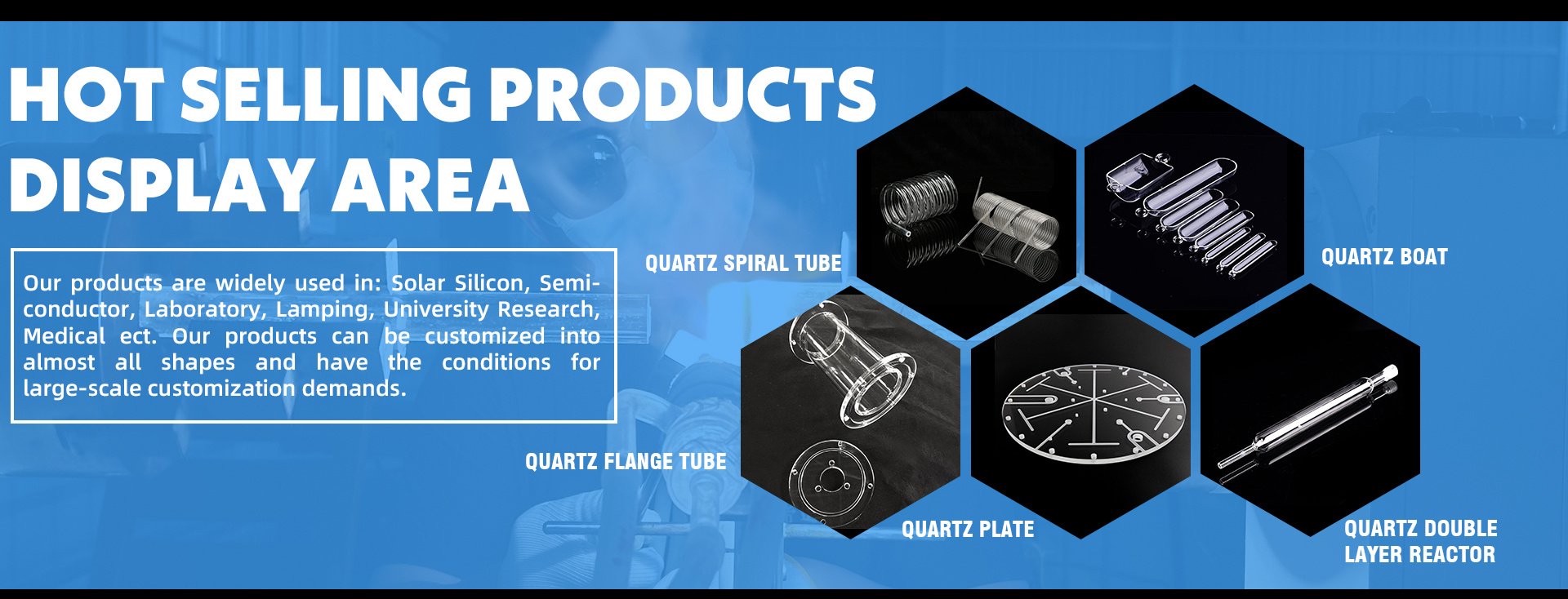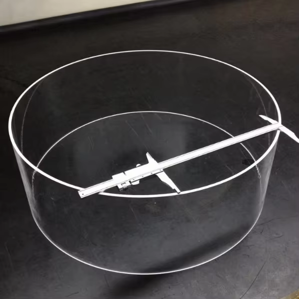
Optical Quartz Sapphire High-Temp Tubes & UV Test Pipes
Purity: >99.99% SiO₂ / Synthetic Al₂O₃
Softening Point: 1683°C (Peak 1750°C)
Working Range: UV-VIS-NIR Spectrum
Explore our core verified fused silica and high-purity quartz portfolio. Fabricated in Donghai with custom OEM/ODM tolerances starting from 1 piece.
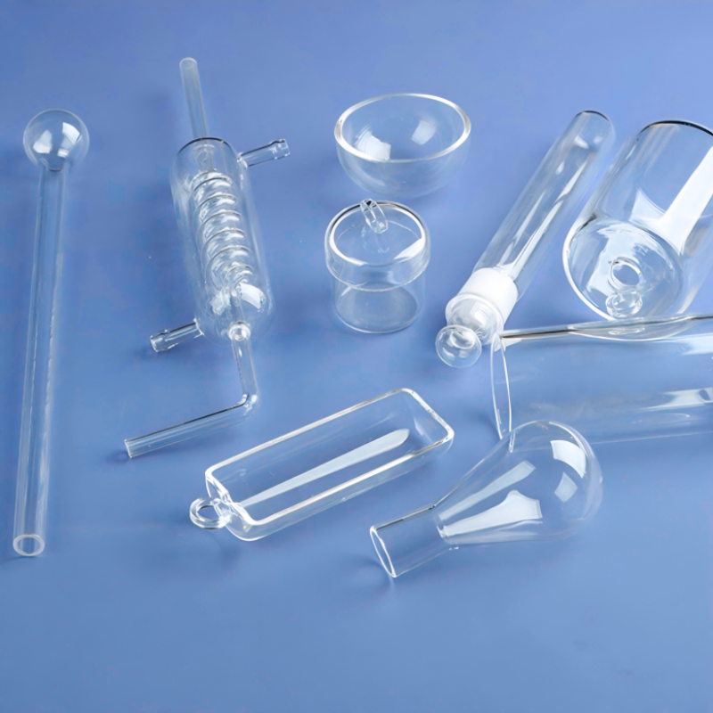
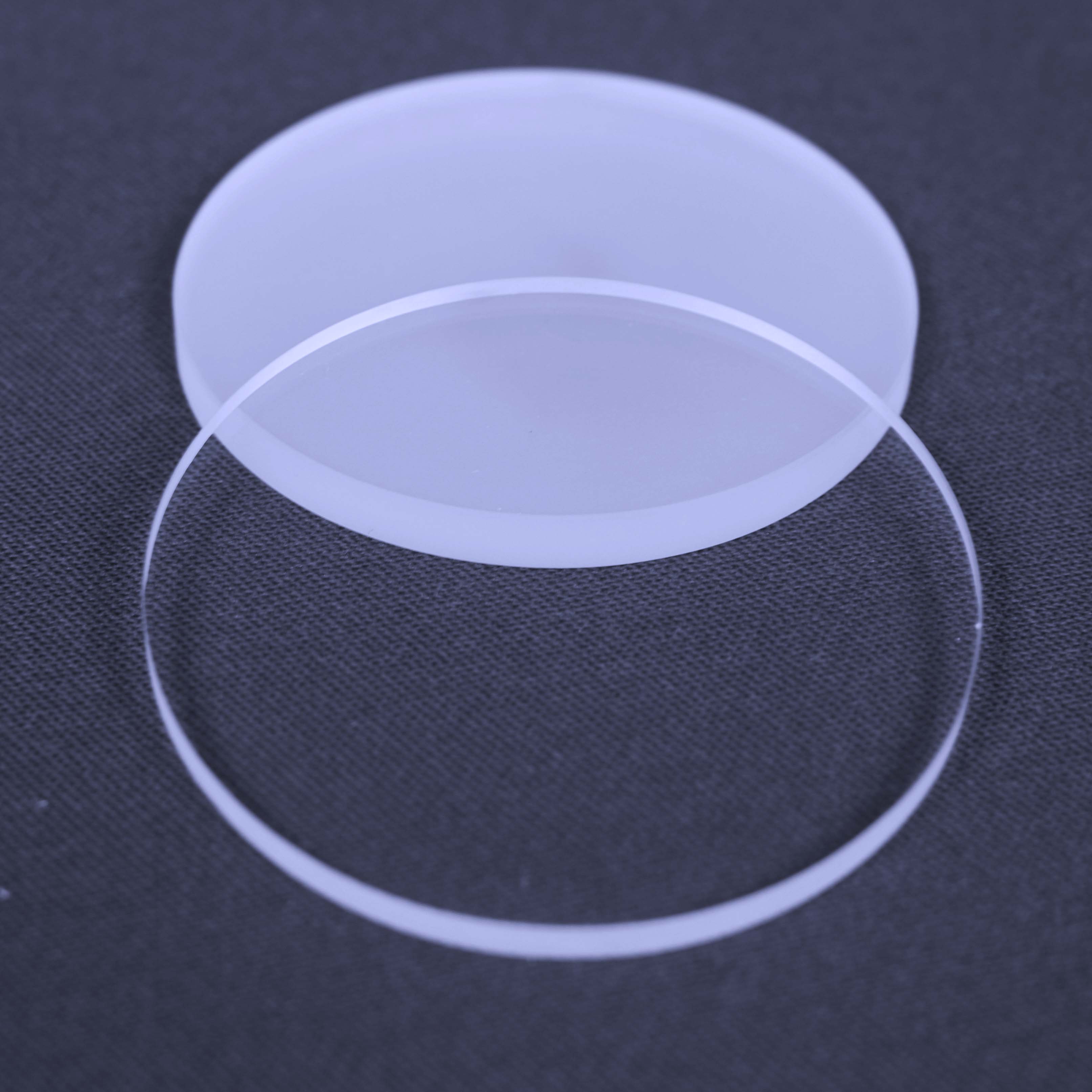
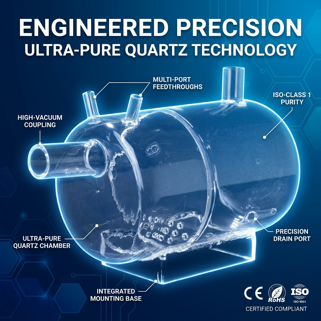
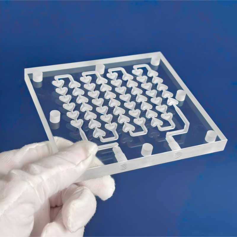
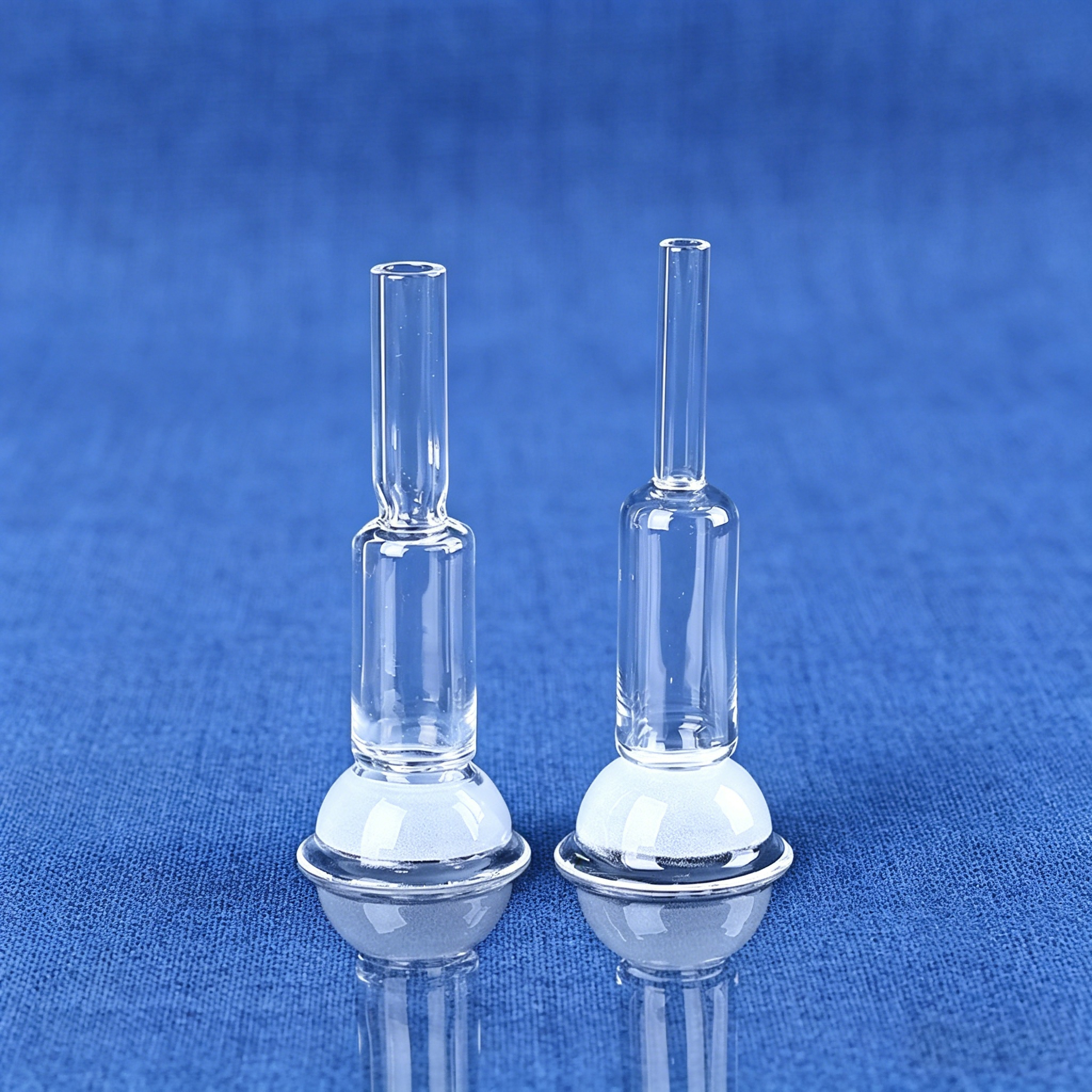
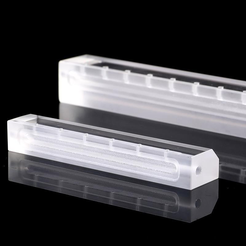
Selecting the optimal quartz substrate requires balancing optical transmittance, thermal expansion coefficients, and chemical impurity profiles across demanding lithography, photonics, and semiconductor environments.
Manufactured via high-purity chemical vapor deposition by reacting silicon tetrachloride (SiCl₄) in an oxy-hydrogen flame. This synthetic method produces an amorphous, isotropic material practically free of metallic impurities (Fe, Al, Ti, Na < 0.1 ppm). It provides unmatched transmission down to the deep ultraviolet (DUV 193nm), zero solarization under excimer laser irradiation, and minimal fluorescence, making it the premier choice for laser optics, photomask substrates, and wafer carriers.
Sourced from high-grade Donghai natural quartz crystal deposits, natural fused quartz is refined through vacuum induction or continuous electric fusion reaching >99.995% to 99.999% purity. It features exceptional thermal shock resistance, an extremely low coefficient of thermal expansion (5.5 × 10⁻⁷ /°C), and negligible bubble inclusions. Natural fused quartz is the industry's cost-effective backbone for high-temperature semiconductor furnace tubes, chemical baths, and infrared windows.
| Substrate Parameter | Synthetic Fused Silica (JGS1 / Suprasil) | Optical Fused Quartz (JGS2 / Infrasil) | Standard Semiconductor Quartz (JGS3) |
|---|---|---|---|
| Primary Optical Range | 185 nm – 2500 nm (Deep UV to Near IR) | 220 nm – 3500 nm (UV to Mid-Infrared) | 260 nm – 3500 nm (Broad Industrial) |
| SiO₂ Chemical Purity | ≥ 99.9999% (< 1 ppm total metals) | ≥ 99.995% (< 15 ppm total metals) | ≥ 99.99% (< 30 ppm total metals) |
| Hydroxyl (OH⁻) Content | High OH (800–1200 ppm) or Low OH (<1 ppm) | Typical OH (30–150 ppm) | Very Low OH (< 5 ppm) |
| Refractive Index (n_d @ 589.3nm) | 1.45840 ± 0.00005 | 1.45845 ± 0.0001 | 1.45850 ± 0.0002 |
| Thermal Expansion (0–300°C) | 5.1 × 10⁻⁷ K⁻¹ | 5.5 × 10⁻⁷ K⁻¹ | 5.5 × 10⁻⁷ K⁻¹ |
| Dielectric Constant (1 MHz @ 25°C) | 3.75 ± 0.05 | 3.78 ± 0.05 | 3.80 ± 0.05 |
| Surface Roughness (CMP Polished) | Ra ≤ 0.2 nm (Super-polished) | Ra ≤ 0.5 nm (Optical standard) | Ra ≤ 1.0 nm (Mechanical polish) |
| Standard Thickness Tolerances | ±0.005 mm (±5 μm) | ±0.02 mm | ±0.05 mm |
Evolving semiconductor chip architectures, micro-optics, and energy transition sectors are fundamentally shifting how global procurement teams source, qualify, and secure high-purity quartz substrates.
As advanced microelectronic packaging surpasses silicon interposer limits, fused quartz and ultra-flat glass substrates are surging. Their high dimensional stability, low dielectric loss, and thermal expansion matching silicon make them pivotal for 2.5D/3D heterogenous integration, AI accelerators, and high-frequency RF front-end modules.
Supply volatility has spurred semiconductor and lab buyers to bypass third-party distributors and partner directly with integrated manufacturers sited within primary geological hubs like Donghai. Direct factory relationships yield up to 35% shorter lead times, audited mineral trace pedigrees, and tight price stability against global raw ingot shortages.
Modern procurement contracts increasingly enforce strict Sub-Surface Damage limits. Micro-cracks induced during wire sawing or coarse lapping propagate under intense laser flux or repeated thermal cycling. Quality engineers now demand non-destructive full-aperture interferometry, confocal microscopy, and HF acid etching test reports before batch signoff.
Rapid iterative cycles in bio-photonics, organ-on-a-chip, and micro-electromechanical systems (MEMS) demand customized geometric substrates without prohibitive standard NRE mold costs. Factories capable of manufacturing drawing-based prototypes starting from 1 unit with 5-day rapid dispatch are winning dominant market share.
Explore the engineering frontiers shaping modern quartz glass substrate manufacturing, including chemical mechanical planarization, ultra-fast laser micromachining, and cleanroom acid annealing.
Traditional wet diamond machining introduces chipping on sub-millimeter quartz channels. Modern manufacturing applies picosecond and femtosecond laser-induced deep etching (LIDE). This process alters the local fused silica glass matrix without heat buildup, enabling aspect ratios > 1:10, taper-free through-glass vias (TGVs), and crack-free microfluidic observation channels.
To eliminate scatter in deep ultraviolet (DUV) optics and quantum photonics, quartz substrates undergo double-sided CMP using stabilized colloidal ceria (CeO₂) slurries. This mechanical-chemical synergy achieves ultra-smooth, atomically flat finishes (Ra ≤ 0.2 nm) with total thickness variation (TTV) < 1 μm across 200 mm and 300 mm fused quartz carrier discs.
Absorption in the infrared (2.73 μm) and laser-induced damage thresholds (LIDT) in high-energy UV laser optics are dictated by internal OH⁻ concentration. Next-generation electrical thermal vacuum degassing lines can reduce OH⁻ levels down to < 1 ppm, virtually eliminating IR attenuation and mechanical hysteresis in critical aerospace sensors.
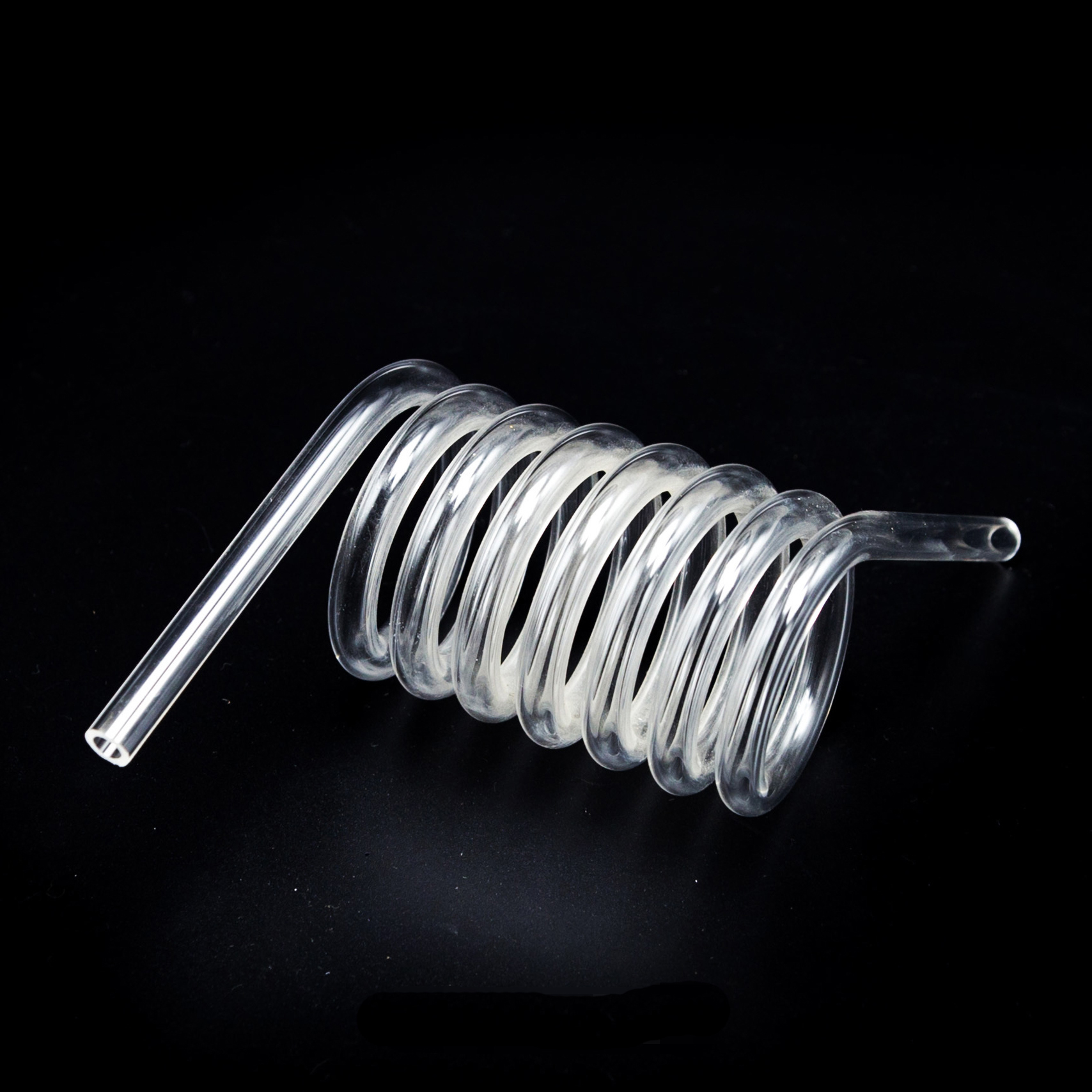
Thermal hot-working, precision tube bending, and seam sealing.
Sub-millimeter dicing with minimal edge chipping and controlled TTV.
Sub-nanometer surface roughness (Ra < 0.5nm) for optical laser discs.
Computer-controlled soaking and cooling to relieve residual stress.
Multi-stage HF/HNO₃ acid cleaning and 18 MΩ·cm DI water rinse.
Laser interferometry, scratch-dig optical rating, and dimensional QC.
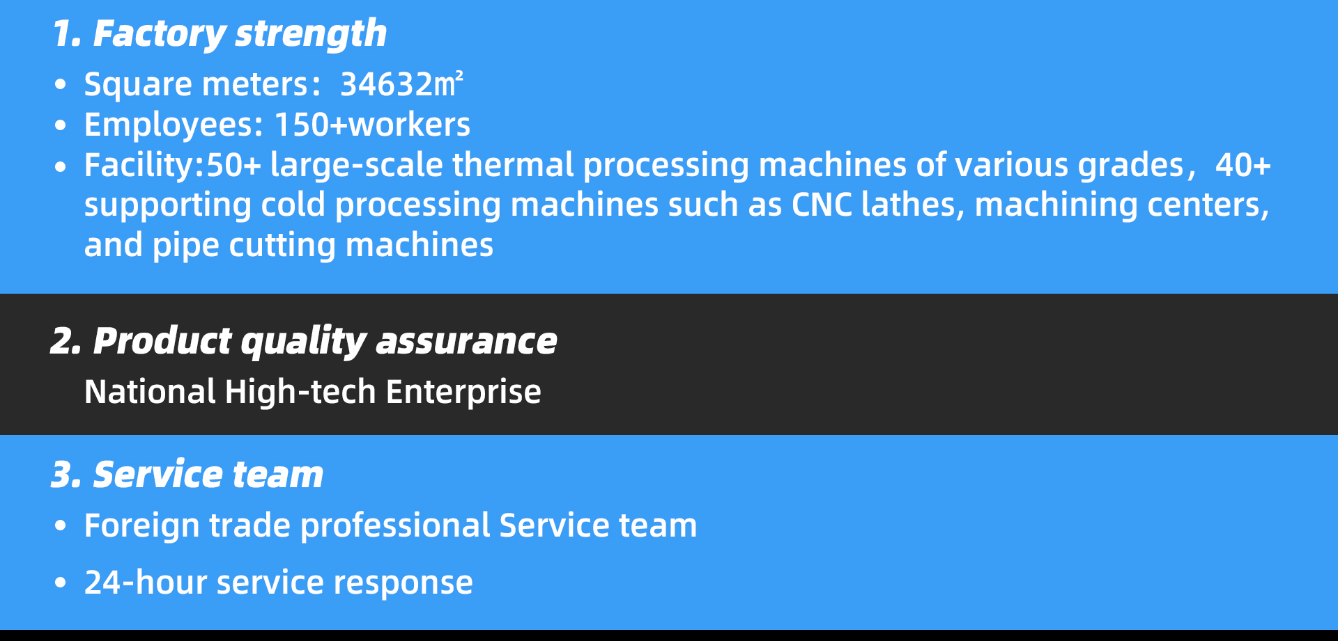
Combining world-class high-purity natural silica sand clusters with vertically integrated hot/cold manufacturing lines and rigorous third-party enterprise verification.
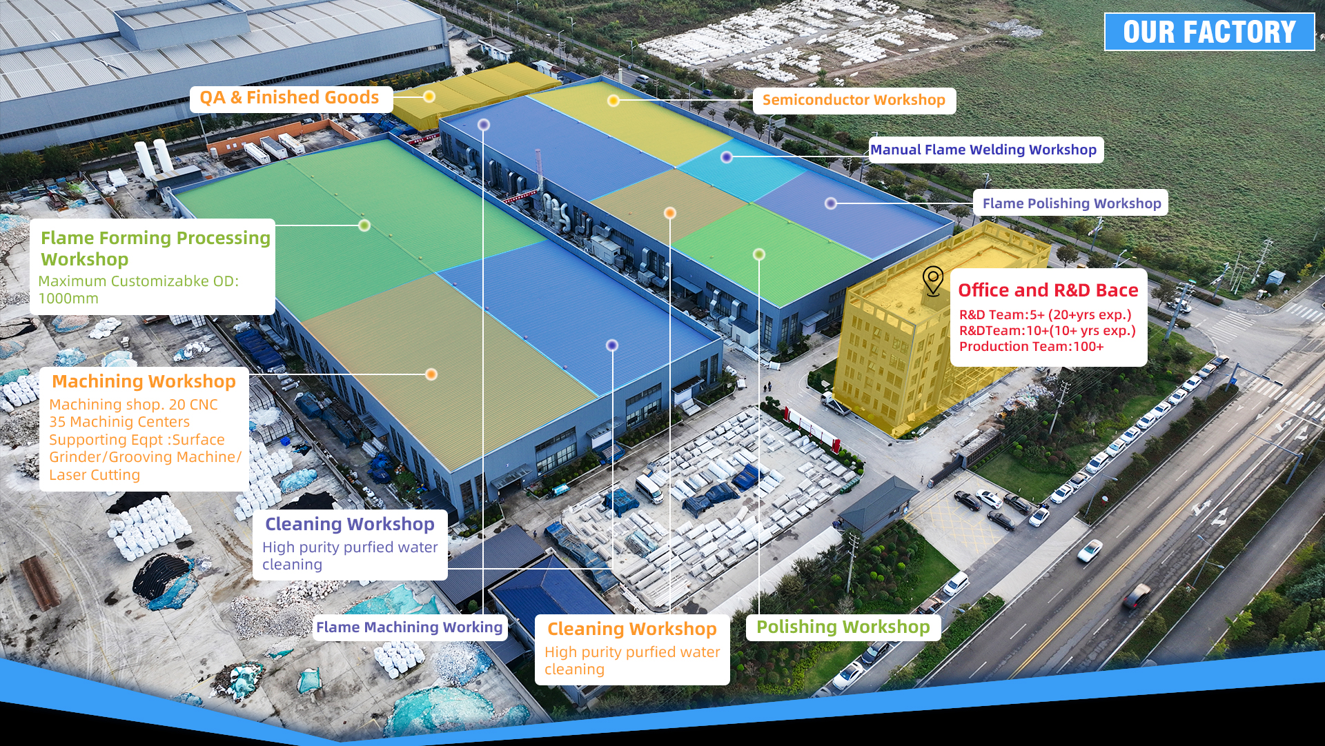
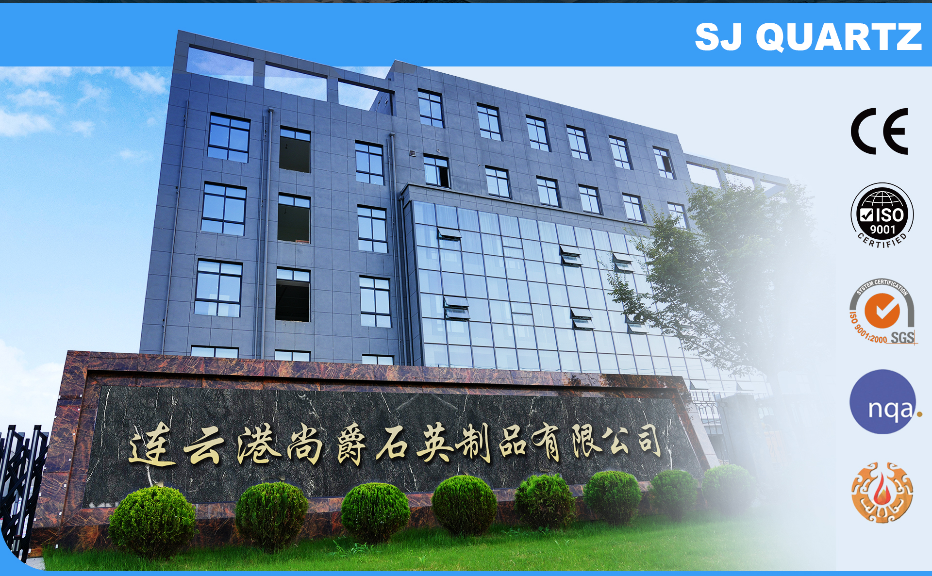
Lianyungang Vulra Quartz Products Co., Ltd. sits at No. 9 Dingxin Road, Jiangsu Donghai Economic Development Zone. Assessed on-site by TÜV Rheinland for production capacity, trade authenticity, and environmental compliance. All our products adhere to CE certification and RoHS environmental directives.


Located in the heart of China’s crystal and quartz cluster, we enjoy immediate raw-material integration, minimizing supply chain intermediaries and providing high-purity quartz sands (SiO₂ > 99.999%) at stable, competitive prices.
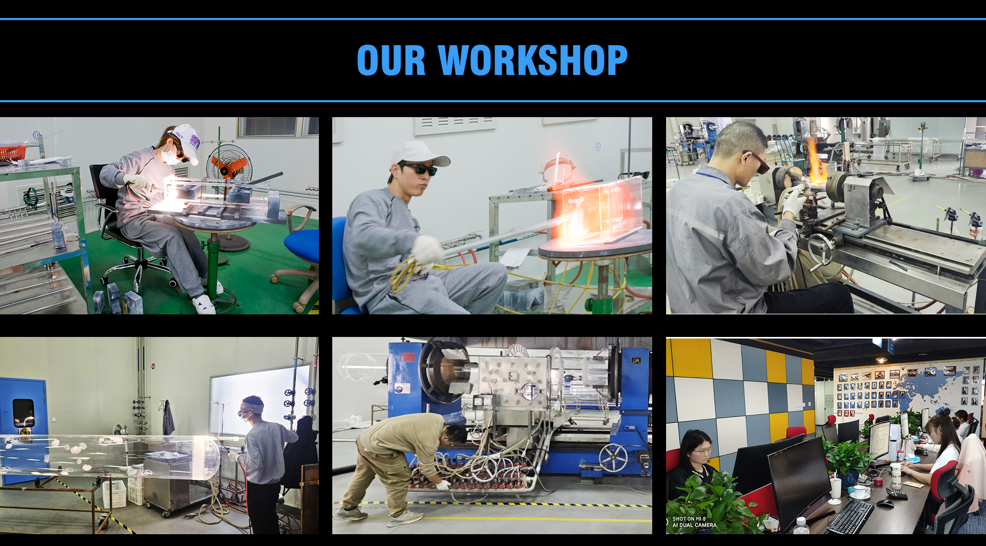
We operate full fabrication workflows under one roof: oxy-hydrogen flame benches, precision glass lathes, diamond wire saws, CNC surface grinders, double-side polishers, ultrasonic drillers, and dedicated annealing chambers.
We respect rapid prototyping cycles. Send your 2D CAD or 3D STEP drawings with custom tolerances, coatings, and geometries. We produce custom substrate runs from single-piece pilot samples to scheduled monthly volume batches.
Fragile quartz requires specialized handling. Every substrate is vacuum-sealed, cushioned with shock-absorbent multi-layer EPE foam inserts, and crated in heavy-duty plywood for complete security during air and ocean freight.
In-depth engineering answers to the critical technical queries raised by optical engineers, cleanroom operators, and international purchasing departments.
Submit your 2D/3D component drawings, target operating temperatures, purity grades, and quantities. Our senior ceramic and quartz fabrication engineers will review your tolerances and provide a prompt quotation.