Featured High-Purity Fused Quartz & Silica Components
Directly sourced from verified raw material reserves and precision hot/cold working lines in Donghai, China.
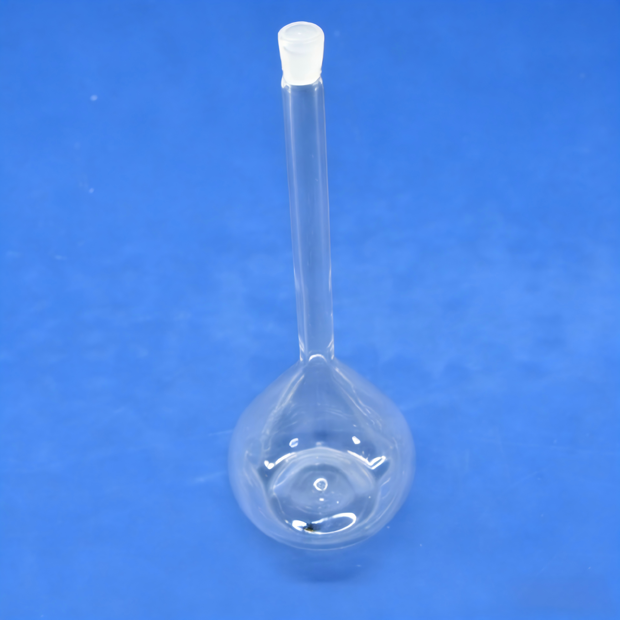
High Purity Transparent Quartz Glass Ampoule & Lab Flask
View Details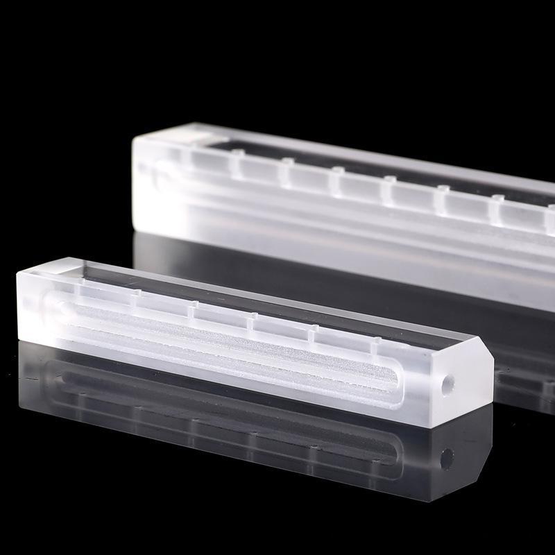
Clear Quartz Testing Sheet Ultra-thin Optical Grade (SJ 077)
View Details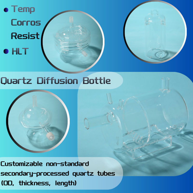
Semiconductor Grade Quartz Purification Units & Condensers
View Details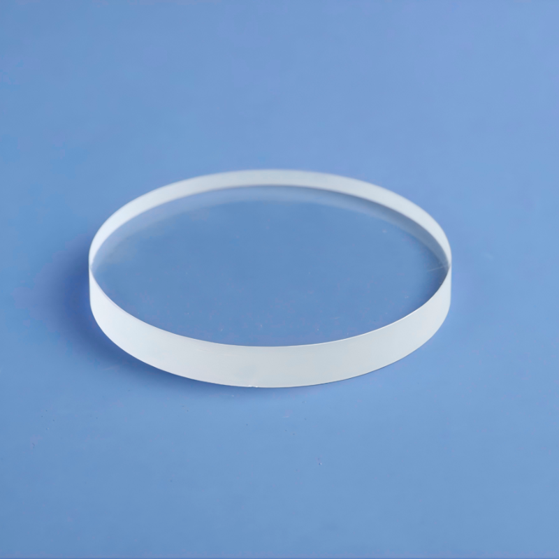
High Temperature Resistant Fused Silica Glass Sheets
View Details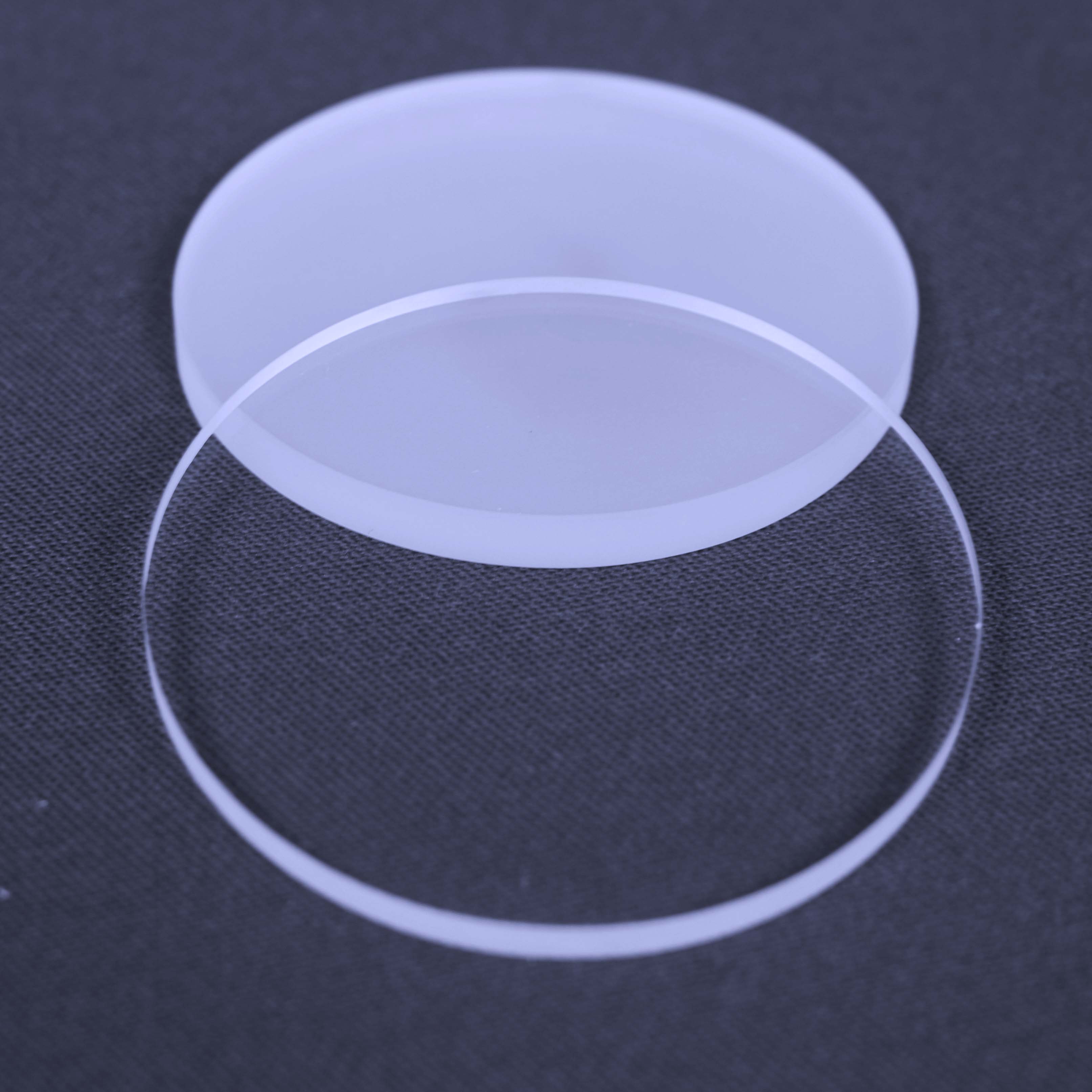
XRD Quartz Holder Test Samples High Transmittance Plate
View Details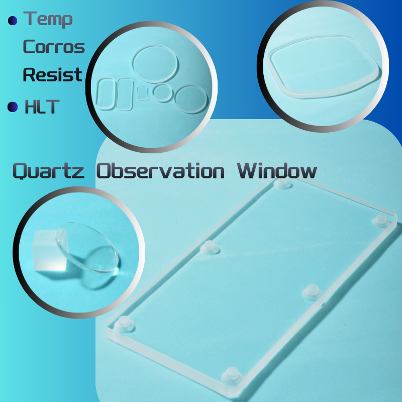
Natural Fused Quartz Polished Plate Optical Clear Heat-Resistant
View Details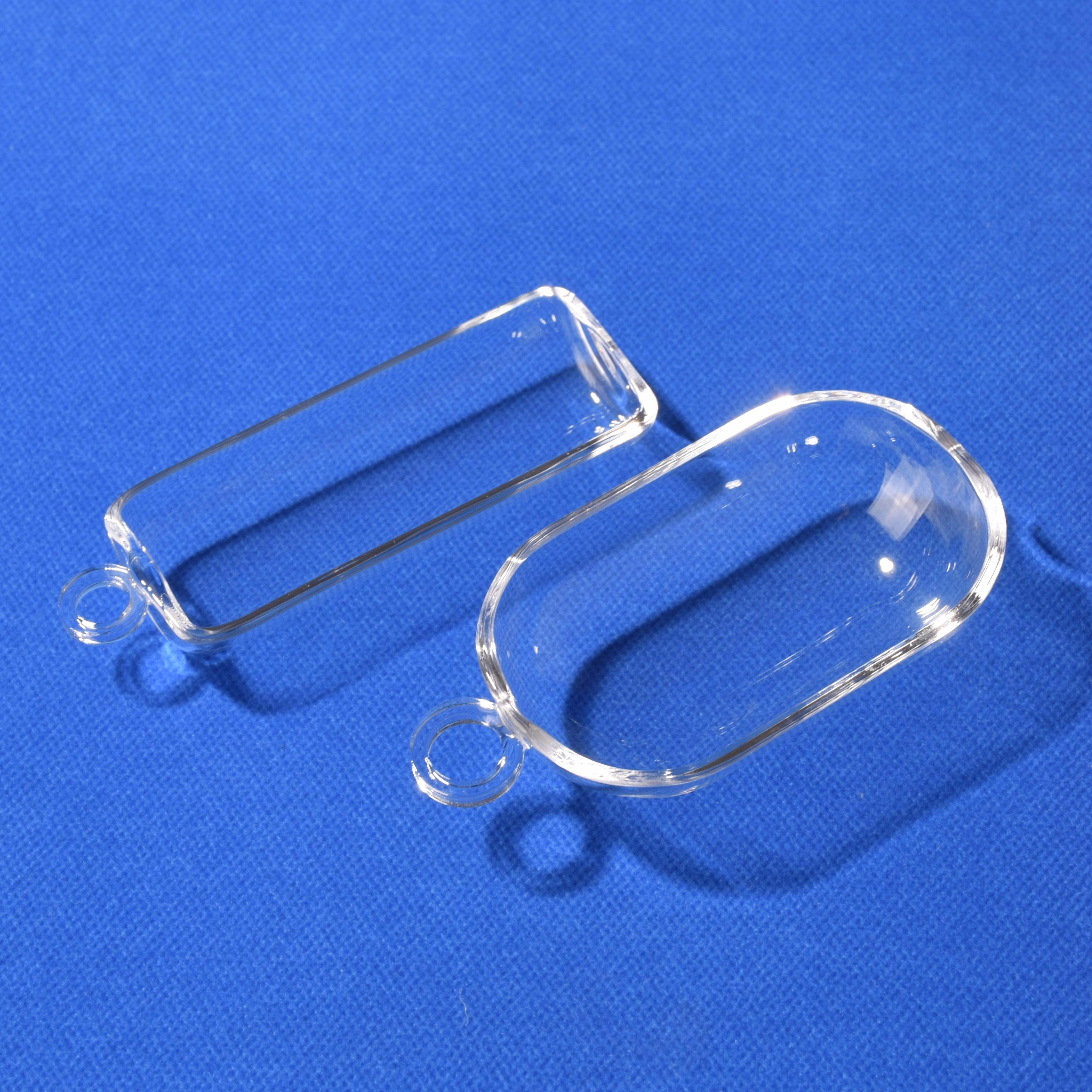
Semi-circular Flat Bottom Tube Furnace Quartz Boat
View Details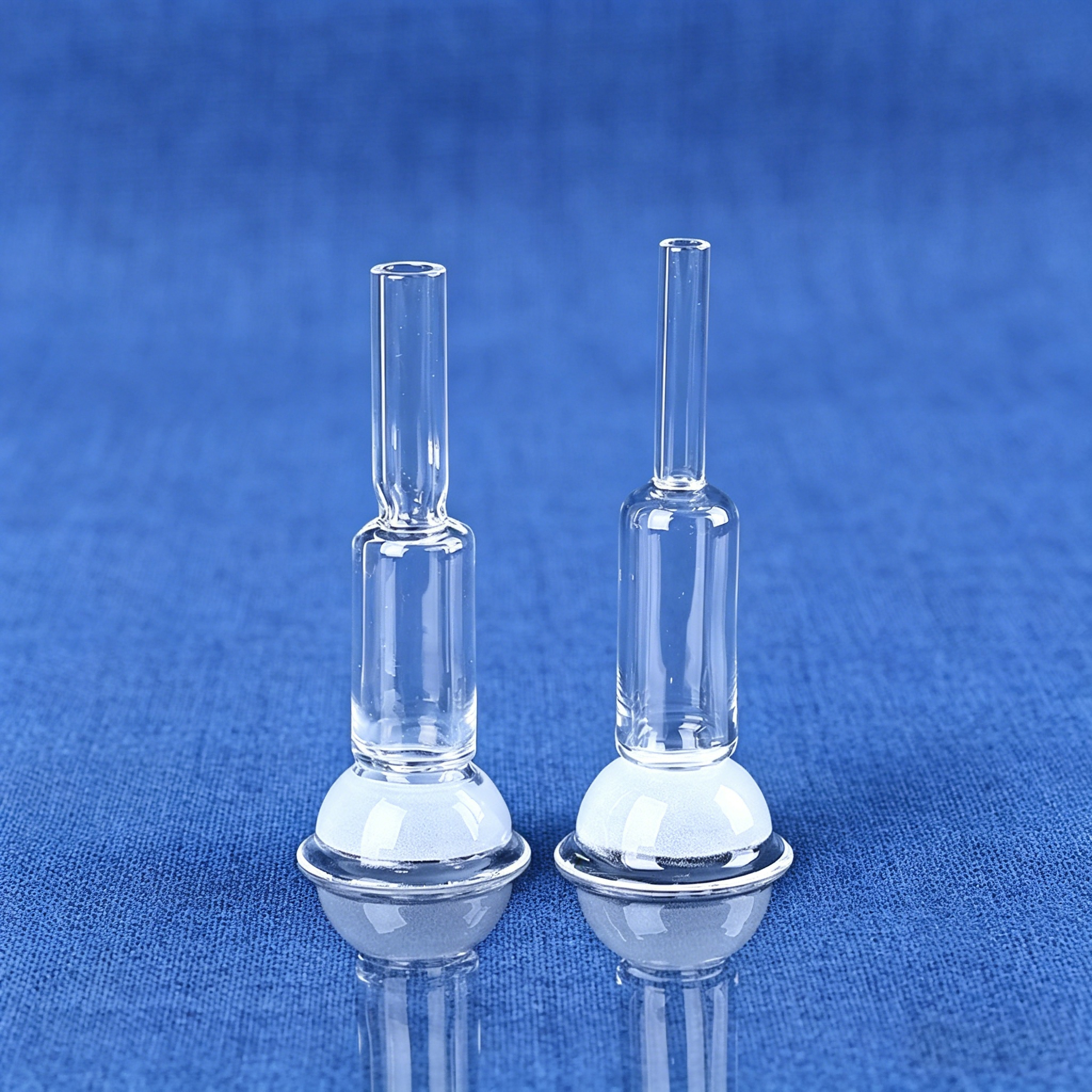
Custom High Purity Quartz C-shaped BET Testing Tube
View Details1. Executive Summary & Global Fused Silica Lump Market Overview
Fused silica lumps represent the fundamental raw building block for high-precision optical components, semiconductor quartzware, photovoltaic crucibles, and specialized laboratory glass. Produced through the controlled ultra-high temperature melting of high-purity quartz crystal sand in specialized electric arc or oxy-hydrogen fusion furnaces, fused silica lumps exhibit an extraordinary combination of mechanical strength, thermal shock resistance, optical transparency, and chemical inertness.
As global high-technology sectors—most notably sub-7nm semiconductor fabrication, N-type TOPCon solar cells, deep-UV optics, and quantum instrumentation—expand exponentially, the procurement standards for raw fused silica lumps have evolved. Procurement officers, process engineers, and technical directors no longer search merely for basic glass suppliers; they require verified, vertically integrated manufacturing partners capable of delivering SiO2 purity levels exceeding 99.999% (5N), with strict micro-ppm trace impurity controls (Fe, Al, Na, K, Li, Ti).
2. Criteria for Ranking Top 10 Fused Silica Lump Factories
To provide B2B buyers with actionable information gain, our engineering evaluation board audited global quartz factories based on six mission-critical operational benchmarks:
Raw Sand Sourcing Control
Direct access to natural pegmatite quartz deposits (such as the Donghai crystal region) or certified high-purity chemical precursor lines to prevent batch-to-batch chemical variance.
Thermal Fusion Technology
Utilization of advanced vacuum electric arc melting and continuous rotary furnaces capable of reaching temperatures >2000°C while preventing micro-bubble inclusion.
Purity Verification (ICP-MS)
In-house Inductively Coupled Plasma Mass Spectrometry (ICP-MS) laboratories ensuring alkali metal impurities remain strictly below total limits of 10-20 ppm.
Custom Cold Working & Machining
Full downstream capability to transform raw fused silica lumps into precision ground grains, optical plates, custom tubes, and furnace boats via diamond cutting and flame polishing.
Third-Party Verification (E-E-A-T)
Independent auditing by international testing bodies such as TÜV Rheinland, CE compliance, and RoHS certifications confirming physical plant facilities and operational integrity.
Agile Supply Chain & Prototyping
Ability to support engineering prototypes from 1 piece up to multi-ton bulk container deliveries with specialized export-ready protective packaging.
3. Material Science Comparison: Natural Fused Quartz vs. Synthetic Fused Silica
A frequent dilemma for procurement teams is selecting between Natural Fused Quartz (derived from natural high-purity lump sand) and Synthetic Fused Silica (synthesized from silicon tetrachloride SiCl4). The table below outlines the physical, optical, and thermal metrics essential for making an informed purchasing decision.
| Property Metric | Natural Fused Quartz Lumps | Synthetic Fused Silica Lumps | Target Industrial Application |
|---|---|---|---|
| SiO2 Purity Level | 99.99% - 99.999% | 99.9999% (6N+) | Semiconductor Furnaces / Deep UV Optics |
| Hydroxyl (OH-) Content | 5 ppm - 50 ppm (Dry) / 150-200 ppm | < 1 ppm (Low OH) or up to 1000 ppm | IR Spectral Windows vs. UV Laser Optics |
| Softening Point (°C) | ~ 1683 °C | ~ 1600 °C | High Temperature Tube Furnaces (1100°C long term) |
| Thermal Expansion Coeff. | 5.5 × 10⁻⁷ / °C (20°C–320°C) | 5.4 × 10⁻⁷ / °C | Ultra-Low Thermal Shock Components |
| Bubble / Inclusion Class | ISO Class 1-3 (Virtually visual bubble-free) | ISO Class 0 (Zero bubble inclusions) | Optical Sight Windows & Substrates |
| Trace Alkali (Na+K+Li) | < 5.0 ppm aggregate | < 0.1 ppm aggregate | Microchip Diffusion Tubes & Wafer Carriers |
Require Custom Fused Silica Lumps or Fabricated Quartzware?
Consult with our engineering team for technical drawing reviews, purity specs, and custom OEM quotes from 1 piece.
4. Future Procurement Trends in the Fused Silica Lump Industry (2025–2030)
Navigating the global quartz supply chain requires anticipating strategic technological shifts. Over the next decade, three dominant trends will dictate how top-tier factories manufacture and price fused silica lumps:
1. Transition to N-Type Solar TOPCon & HJT
Photovoltaic wafer manufacturing is rapidly abandoning older P-type PERC tech for N-type TOPCon. This shift demands quartz crucibles and continuous feeding tubes made from higher purity fused silica lumps to eliminate alkali metal migration that reduces solar cell efficiency.
2. Sub-3nm Semiconductor Wafer Demands
As semiconductor node sizes shrink below 3nm, micro-contamination during oxidation and diffusion steps becomes unacceptable. Wafer fab operators are mandating low-hydroxyl, low-boron fused silica tube assemblies produced from ultra-refined synthetic and natural lump stock.
3. Circular Economy & Recycled Fused Quartz
Leading factories are implementing closed-loop cleaning processes to crush, acid-wash, and re-fuse clean quartz scrap into secondary structural lumps, reducing the carbon footprint of high-energy electric melting operations by up to 25%.
5. Enterprise Advantage: Lianyungang Vulra Quartz Products Co., Ltd.
Headquartered in Donghai County—the recognized "Crystal Capital of China"—Lianyungang Vulra Quartz Products Co., Ltd. stands as an industry benchmark among top fused silica glass manufacturers. Verified on-site by third-party inspection powerhouse TÜV Rheinland, Vulra Quartz operates a complete, integrated production chain spanning raw material refining, flame lathe working, cold diamond grinding, cleanroom acid washing, and optical polishing.
Why Global Buyers Choose Vulra Quartz for Fused Silica Products:
- ✔ Location Advantage: Immediate proximity to Donghai’s raw crystal and high-purity quartz sand reserves ensures stable pricing and uncompromised supply continuity.
- ✔ Engineering First OEM/ODM: Support for drawing-based custom processing with zero minimum order quantity (MOQ 1 PC for custom plates, boats, and crucibles).
- ✔ Stress Relief Annealing: Every hot-worked tube, flask, or furnace boat undergoes computer-controlled thermal annealing to eliminate internal stress birefringence and prevent shattering during thermal cycling.
- ✔ Export Packaging: Dedicated multi-layer shock-absorbing foam and reinforced sea/air freight wooden crates designed specifically for fragile glass transportation.
6. Frequently Asked Questions (Procurement FAQ)
Key technical answers curated by our senior material engineers to streamline your sourcing workflow.
Ready to Accelerate Your Quartz Supply Chain?
Send your drawings or bulk fused silica lump specifications today for a detailed engineering response within 24 hours.