Custom Clear Fused Quartz Tube / High-Purity Vessel SJ 226
Fire-polished fused silica with near-zero bubble density. Outstanding chemical resistance for high-temperature diffusion and wafer chemical processing.
Engineered from natural pegmatite quartz in Donghai, each component undergoes stringent vacuum thermal annealing, acid etching, and ISO Class 5 DI-water ultrasonic cleaning to ensure ultra-low particle generation in critical semiconductor vacuum chambers.
Fire-polished fused silica with near-zero bubble density. Outstanding chemical resistance for high-temperature diffusion and wafer chemical processing.
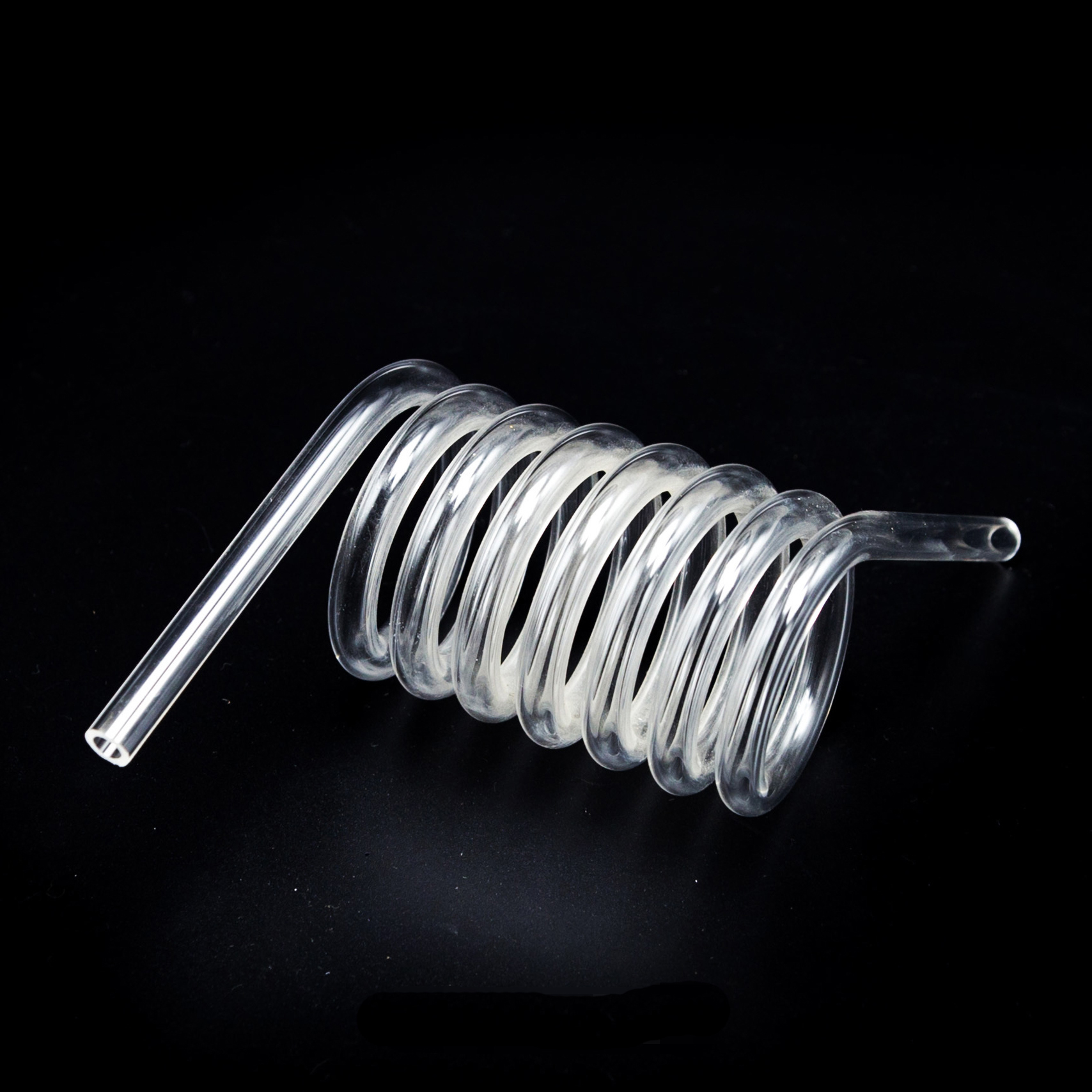
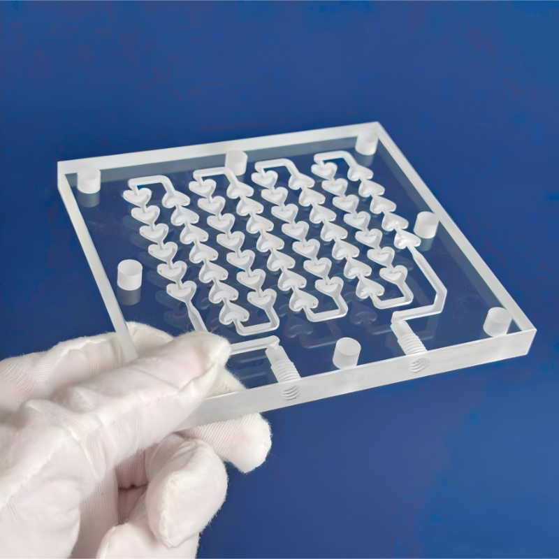
Micro-tolerance plasma-lathe bending and cold diamond cutting. Designed for specialized gas injection lines, chamber bypass manifolds, and heating spirals.
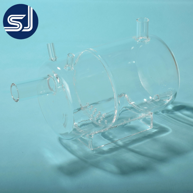
Continuous operation at 1100°C. Optical transmission >85%, exceptional resistance against corrosive fluorine and chlorine etch exhaust effluents.
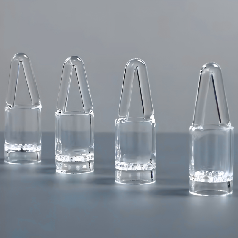
Heavy-wall fused quartz basket with closed-end dome design. High tensile strength of 48 N/mm² optimized for wet bench wafer cleaning chemistry.
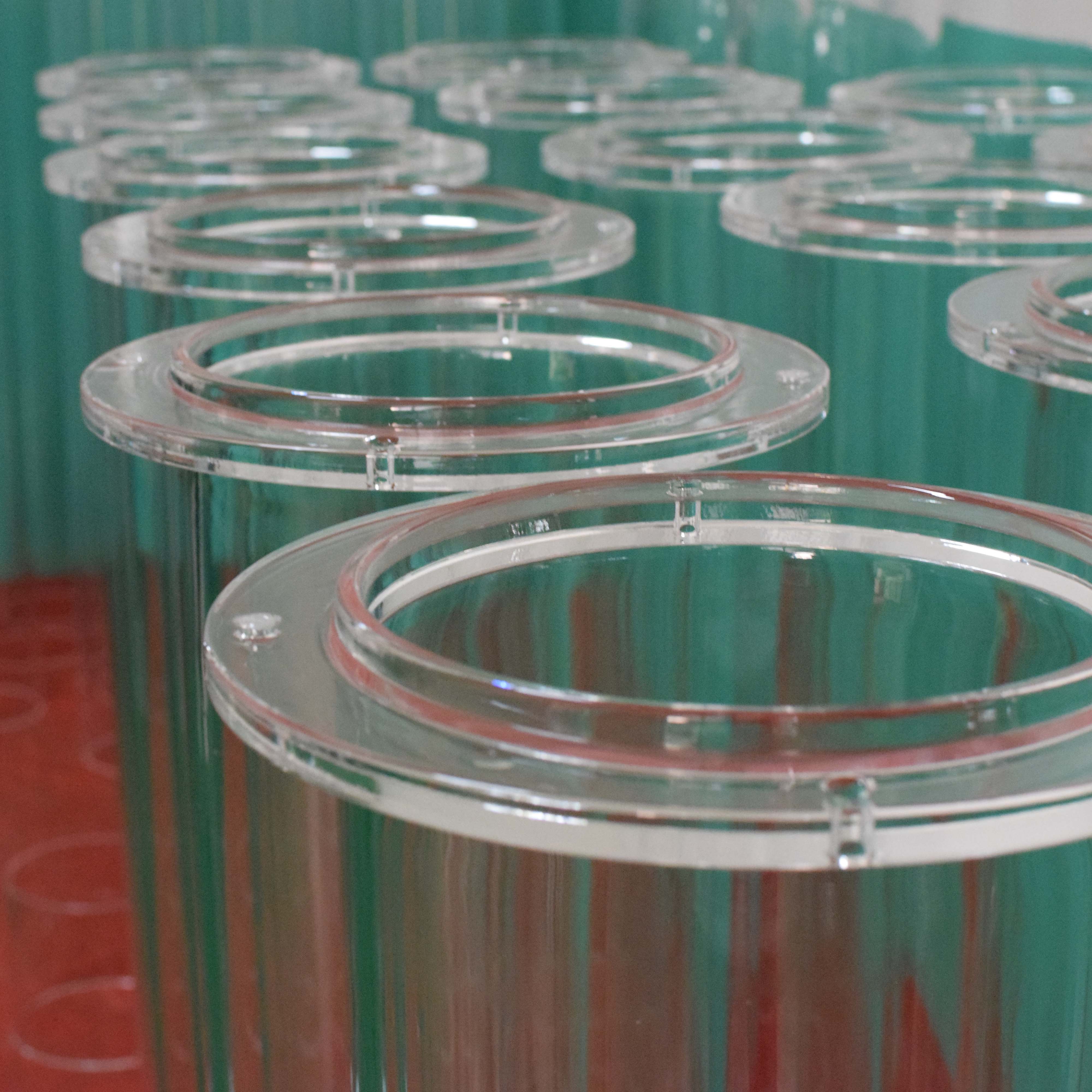
Ultra-pure semiconductor grade fused silica flange ring. Precision diamond ground mating surface for high-vacuum LPCVD and EPI furnace sealing.
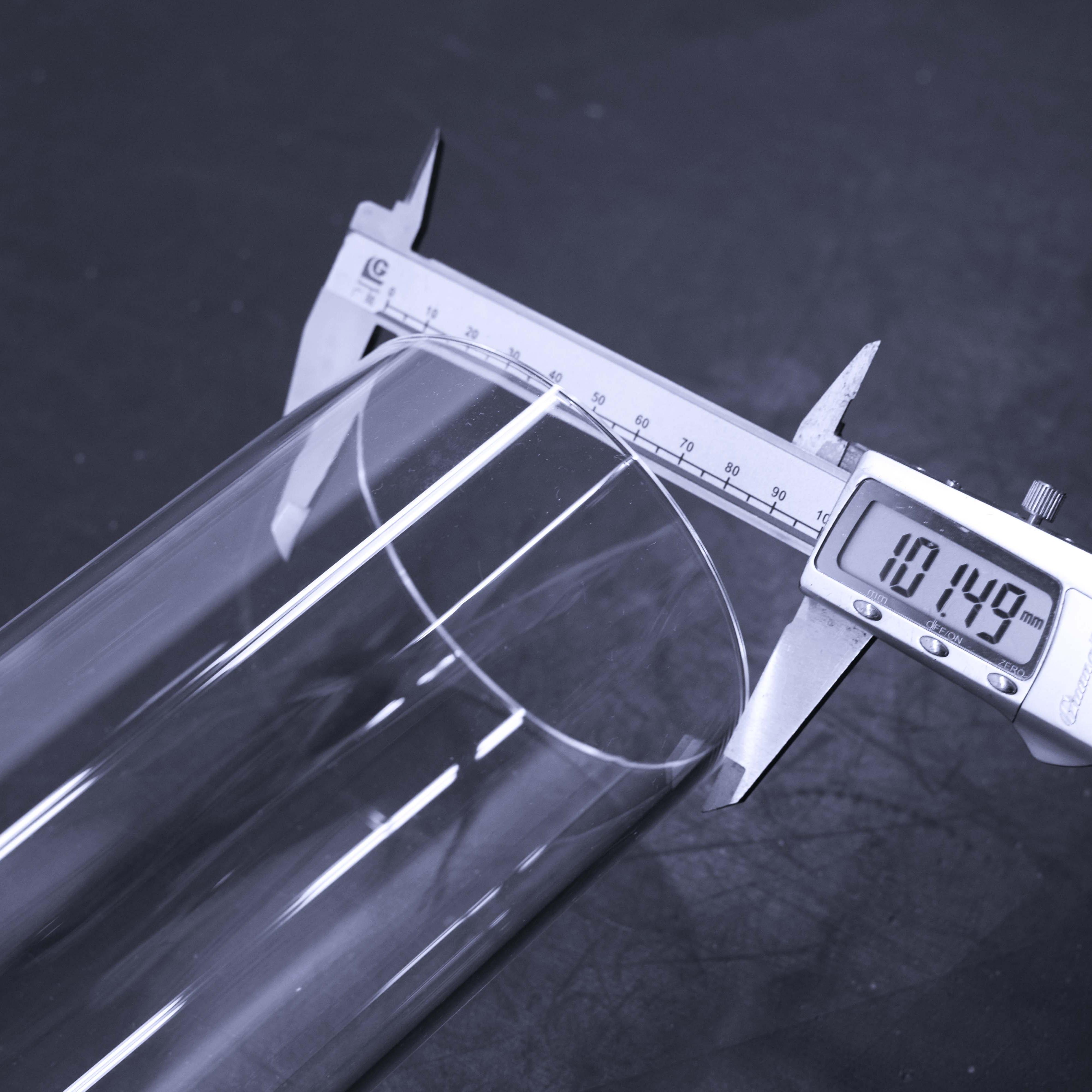
Custom outer diameters from 5mm to 800mm. Exceptionally low thermal expansion (CTE 5.5×10⁻⁷/°C) for thermal process chambers and focus ring preforms.
1750°C melting point quartz interlayer discs. Specially optimized thermal dissipation profile for high-density plasma etch chuck backing plates.
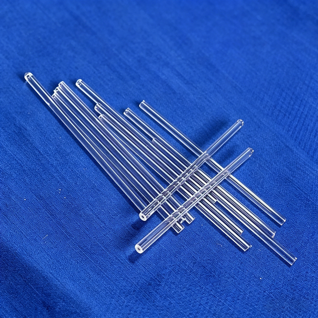
2-10mm precision outer diameter with uniform micro-bore bore tolerance. Used for gas sampling probes, precursor delivery, and thermal sensor sheaths.
In ultra-clean semiconductor wafer fabrication, the wafer edge represents one of the most volatile physical interfaces in modern plasma etching, chemical vapor deposition (CVD), and physical vapor deposition (PVD) processes. A semiconductor quartz ring—frequently configured as a focus ring, shadow ring, clamp ring, or quartz chamber liner—is not merely a passive structural housing; it is an electrically and thermally critical boundary component that directly defines plasma sheath uniformity, edge-die yield, and chamber mean-time-between-cleans (MTBC).
As integrated circuit (IC) architectures progress into 3nm and below, utilizing FinFET, Gate-All-Around (GAA) nanosheets, and multi-tier 3D NAND with 200+ vertical layers, the physical demands placed on quartz consumable components have amplified drastically. Fabs can no longer tolerate micro-fissures, uncontrolled hydroxyl (OH⁻) content, or alkali metal outgassing. Lianyungang Vulra Quartz Products Co., Ltd., situated directly within China's primary silica hub of Donghai, manufactures and exports CE-certified, TÜV Rheinland-verified semiconductor quartz rings designed to maintain sub-micron dimensional stability under relentless RF plasma bombardment.
Our CE-marked semiconductor quartz rings are manufactured from electric-fused or gas-fused natural quartz crystal sand (99.999% SiO₂) as well as synthetic fused silica precursors. The following matrix illustrates the verified physical, electrical, and chemical benchmarks certified across our global export shipments:
| Physical & Chemical Parameter | Semiconductor Grade (Vulra 5N) | Optical / Chamber Grade (Vulra 4N) | Standard Lab Glass (Borosilicate Ref.) |
|---|---|---|---|
| Chemical Purity (SiO₂ Content) | ≥ 99.999% (5N Ultra-Pure) | ≥ 99.99% (4N Industrial) | 80.5% ± 1.0% (Inadequate for Fabs) |
| Total Trace Metals (Al, Fe, Ti, Ca, Mg, Na, K, Li) | ≤ 5.0 ppm Total (Alkali ≤ 0.8 ppm) | ≤ 18.0 ppm Total | > 25,000 ppm (Contaminates Gates) |
| Hydroxyl Radical (OH⁻) Concentration | < 5 ppm (Dry Gas-Fused Option) | < 30 ppm (Standard Electric Fused) | Uncontrolled / Variable |
| Coefficient of Thermal Expansion (20–300°C) | 5.5 × 10⁻⁷ / °C | 5.5 × 10⁻⁷ / °C | 33 × 10⁻⁷ / °C (6x Higher Hysteresis) |
| Continuous Working Temperature Limit | 1150 °C | 1100 °C | 500 °C |
| Softening Point (Log η = 7.6) | 1683 °C | 1680 °C | 820 °C |
| Dielectric Strength (20°C, 1MHz) | 25 – 40 kV/mm | 20 – 30 kV/mm | 10 kV/mm |
| Machining Precision & Flatness | ± 0.02 mm / Flatness ≤ 0.01 mm | ± 0.05 mm | ± 0.20 mm |
| CE & RoHS Compliance Status | Fully Certified & Traceable | Fully Certified | Basic Industrial Only |
Global semiconductor foundries and Integrated Device Manufacturers (IDMs) are restructuring their quartz procurement playbooks. As geopolitical dynamics, wafer scaling, and total cost of ownership (TCO) converge, procurement directors must anticipate four macro sourcing shifts.
Procurement is no longer judged solely on initial part unit cost. A focus ring failure or premature replacement requires a chamber breach, multi-hour cool-down, pump-down, re-qualification wafers, and thousands of dollars in lost fab throughput. High-purity, vacuum-annealed quartz rings that extend chamber service intervals from 180 RF hours to 280+ RF hours deliver vastly superior net economic returns.
Lead times for OEM-branded chamber quartz (Applied Materials, Lam Research, Tokyo Electron) frequently stretch beyond 30 to 52 weeks during chip super-cycles. Tier-1 foundries are aggressively validating independent, drawing-to-spec manufacturers like Vulra Quartz as dual-source qualified vendors. Complete dimensional, chemical, and plasma-behavior parity is mandatory under strict change-of-control protocols.
High-purity quartz sand is an internationally strategic material. Having manufacturing operations embedded within Donghai—the world center for quartz crystallization and refining—provides Vulra Quartz uninterrupted access to high-grade crystalline feedstock. This geographic synergy insulates overseas buyers from upstream supply shocks and severe logistics delays.
European and North American fab expansions mandate strict environmental compliance under EU RoHS (2011/65/EU) and REACH frameworks. Fabs increasingly demand certified non-hazardous processing, fluorinated acid neutralization during etching, and full traceability of quartz raw material origins to satisfy modern ESG governance audits.
The transition from planar CMOS to 3D FinFET, nanosheet GAA architectures, and back-side power delivery networks (BSPDN) has radically elevated chamber processing parameters. Quartz components are no longer subjected to moderate thermal cycles; they endure extreme high-density plasma fluxes, cryogenic dry etch regimes (-60°C), and high-temperature atomic layer deposition (ALD) chemistry. Below are the definitive technological evolutions shaping quartz ring engineering:
Traditional mechanical grinding and diamond-blade cutting inevitably introduce microscopic sub-surface micro-cracks (SSD) extending 10 to 50 μm beneath the quartz surface. Under repeated thermal shock cycles (20°C → 1100°C) and aggressive plasma etching, these micro-cracks propagate, leading to catastrophic particle spalling and wafer contamination. Next-generation quartz ring suppliers must deploy multi-axis ultrasonic grinding combined with controlled hydrofluoric (HF) acid chemical polishing. This removes the fractured amorphous layer, leaving an ultra-smooth, crack-free surface with surface roughness values of Ra ≤ 0.2 μm.
The molecular configuration of fused quartz significantly dictates its performance under plasma assault. High-hydroxyl quartz (>150 ppm OH⁻) exhibits lower viscosity and is highly prone to structural sagging and rapid dry-etch erosion when exposed to fluorine-based energetic ions. For dry etch and high-temperature LPCVD applications, Vulra Quartz produces gas-refined, low-OH⁻ quartz rings (<5 ppm OH⁻) that demonstrate superior mechanical rigidity and reduced chemical reaction kinetics with CF₄/SF₆ plasmas.
In high-aspect-ratio (HAR) contact etch processes for 3D NAND, conventional quartz rings erode rapidly, necessitating replacement every few weeks. Cutting-edge research involves doping quartz substrates with rare-earth oxides (such as Y₂O₃ yttrium oxide) or thermal-spraying yttria-alumina-garnet (YAG) barrier coatings onto the plasma-exposed quartz faces. These advanced barriers reduce the physical sputtering yield by up to 70%, prolonging component longevity in extreme halocarbon plasma chambers.
Lianyungang Vulra Quartz Products Co., Ltd. operates an integrated, audit-ready manufacturing campus in the Jiangsu Donghai Economic Development Zone. As a TÜV Rheinland-verified custom manufacturer, we unite geological raw material dominance with pristine cleanroom machining.
Directly headquartered in China's quartz capital, Vulra Quartz sources purest natural silica sands at predictable costs. We maintain vast stockpiles of raw ingots, bypassing intermediary markups and ensuring dependable supply chain velocity.
Our workshop merges oxy-hydrogen flame manipulation, custom automated glass lathes, multi-axis CNC milling, diamond wire slicing, ultrasonic drilling, and computerized optical surface polishing within a single facility.
Our operational capabilities, corporate legal status, trade compliance, and precision machinery have been comprehensively inspected and confirmed by TÜV Rheinland. We maintain ISO-equivalent clean handling and documented QA traceability.
Whether you require a single 1-piece specialized prototype for an experimental pilot line or recurrent monthly batches of 500+ precision focus rings, our application engineering team reviews every CAD tolerance and stress contour before manufacturing.
Detailed technical, quality, and logistics insights addressing the most critical vetting questions asked by foundry supply chain managers and chamber maintenance engineers.
Request our comprehensive semiconductor quartzware engineering manual, material impurity certificates, and OEM dimensional catalogs. Rapid quotation and drawing feasibility reviews within 24 hours.
Get Catalog