Featured Quartz Products for Kobe High-Tech Facilities
Custom OEM/ODM precision fused silica components engineered to tight dimensional tolerances, certified for extreme thermal stability up to 1450°C and zero ionic contamination.
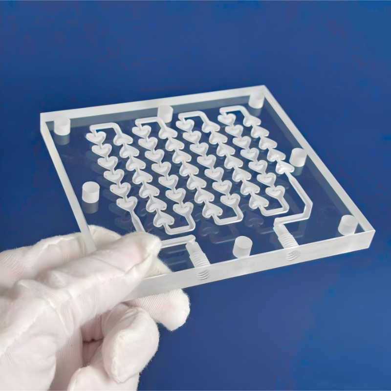
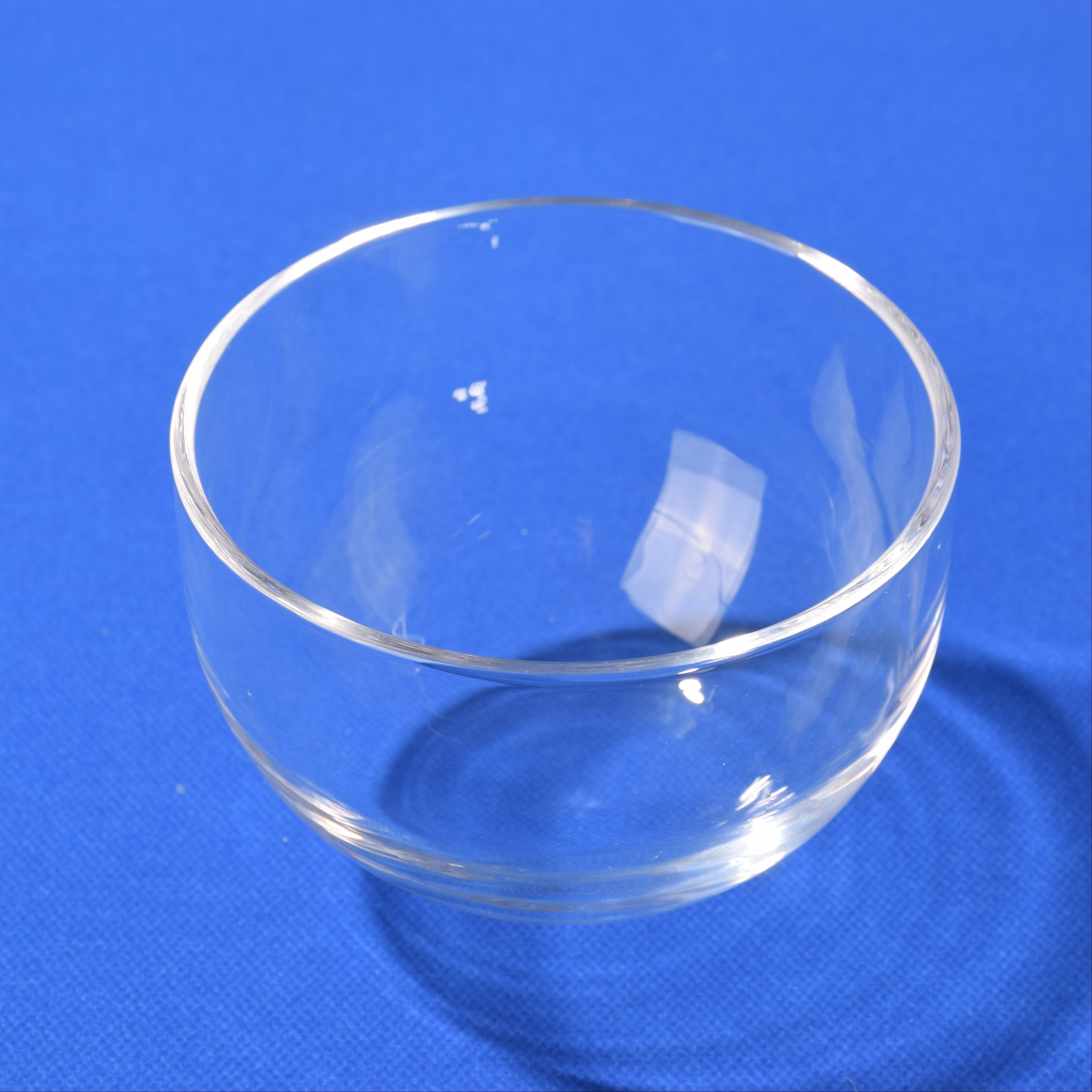
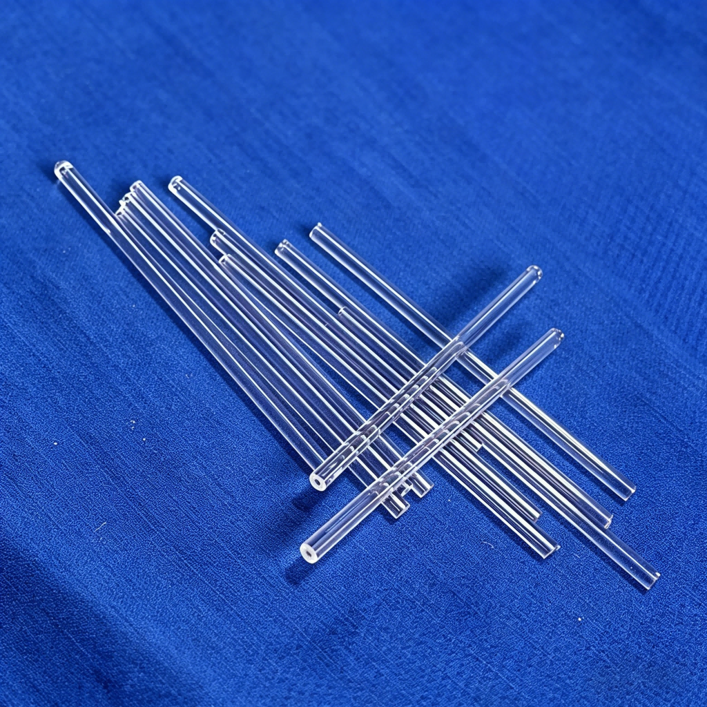
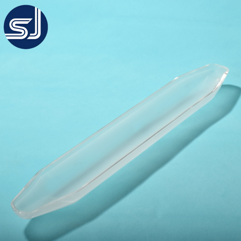
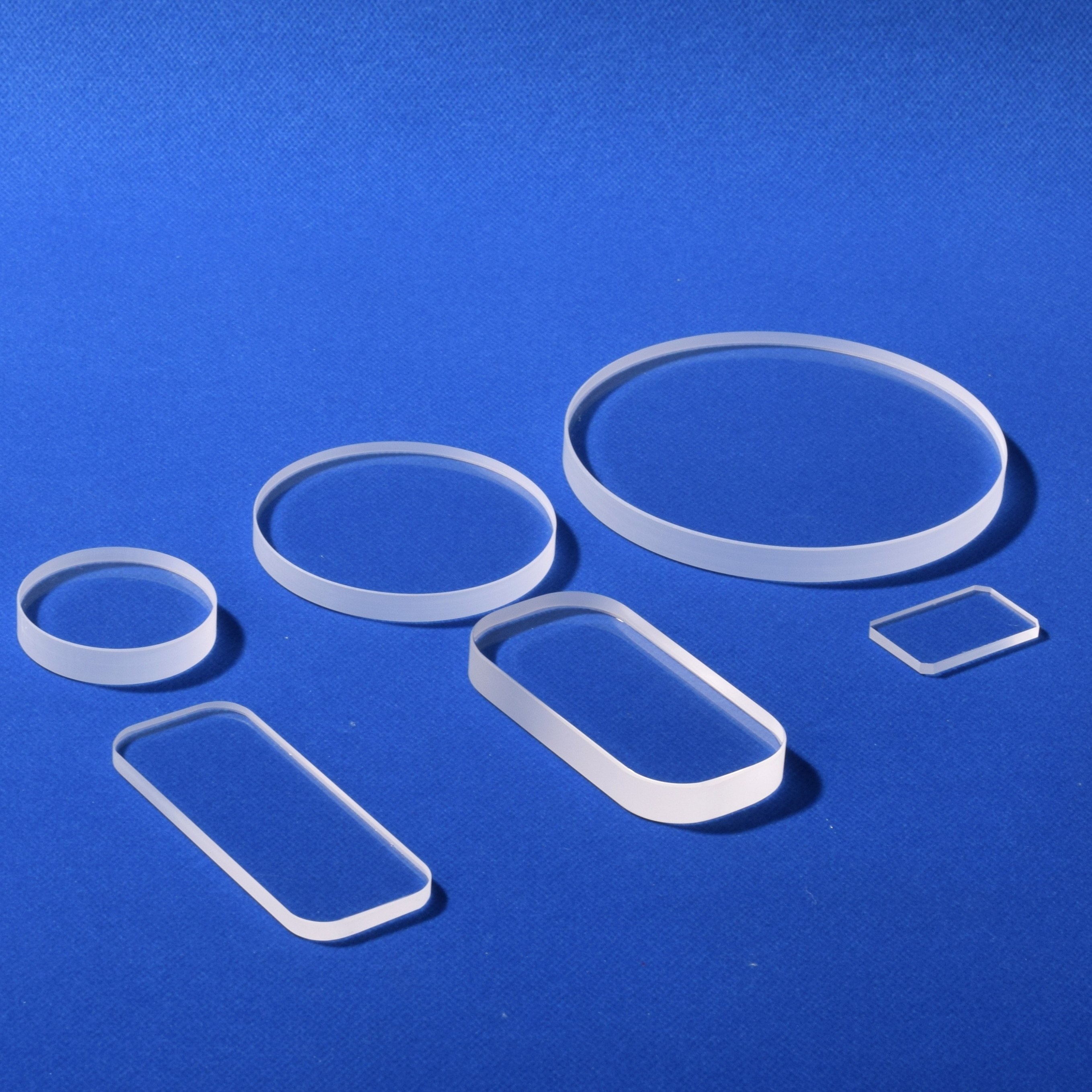
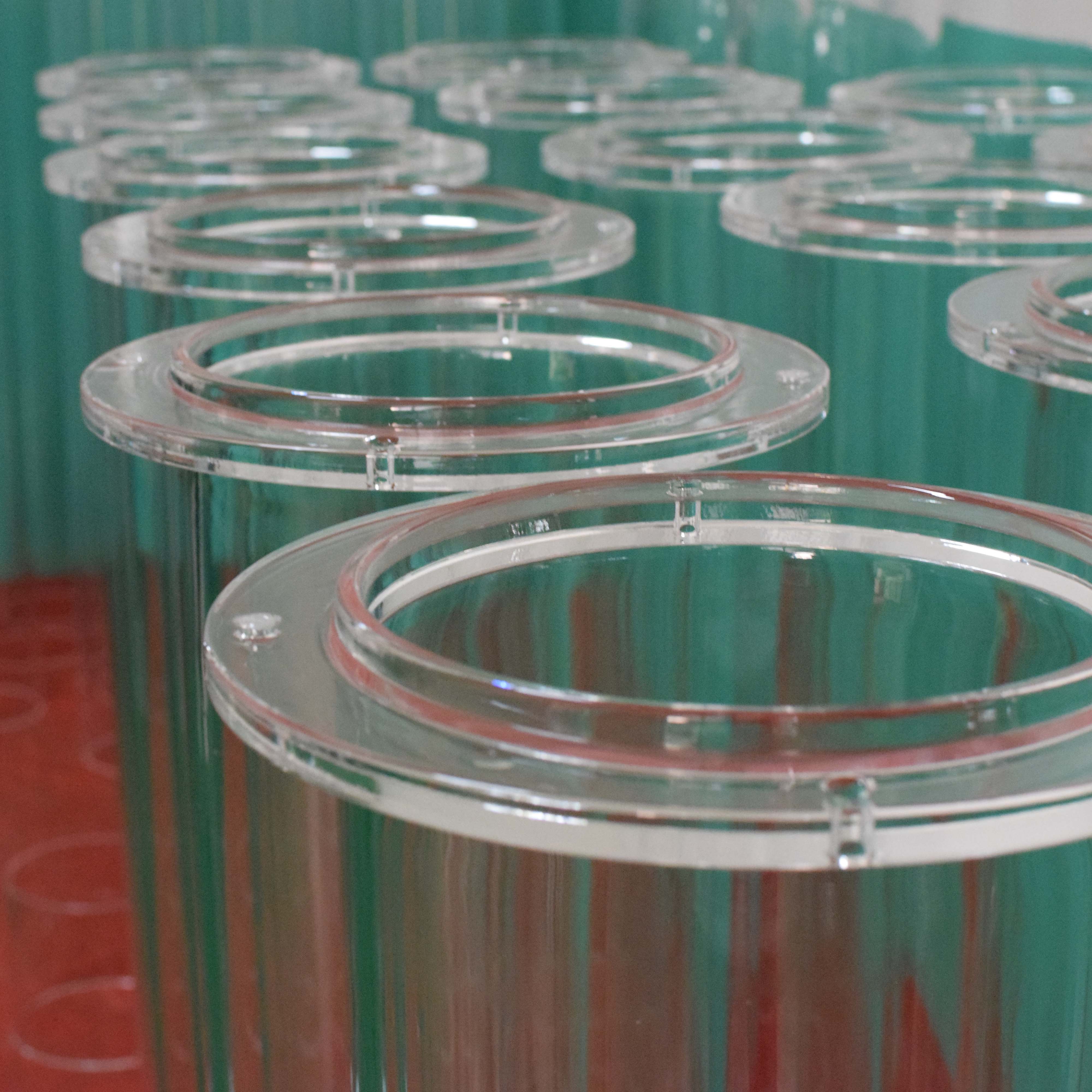
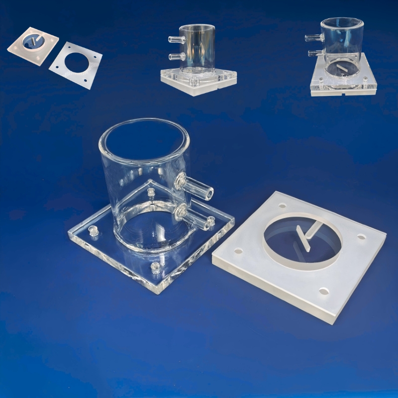
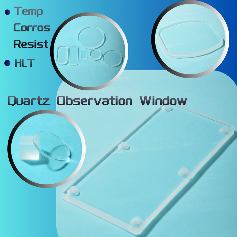
Engineering Quartz Wafer Boats for Next-Generation Thermal Processing in Kobe
As the semiconductor corridor of the Kansai region accelerates its transition toward wide-bandgap (WBG) microelectronics, power discretes, and specialized photonic components, wafer carrier integrity has become a primary bottleneck in furnace yield optimization. Kobe’s engineering ecosystem—spanning the historic industrial maritime sector, advanced nanotechnology research institutes on Port Island, and nearby semiconductor packaging and fabrication facilities—requires thermal handling fixtures capable of sustaining extreme thermal stress without particulate shedding, structural sagging, or atomic cross-contamination.
A quartz wafer boat, also referred to as a fused silica wafer carrier or diffusion cradle, serves as the mechanical backbone within horizontal diffusion tubes, low-pressure chemical vapor deposition (LPCVD) chambers, and rapid thermal oxidation furnaces. Because silicon, silicon carbide (SiC), and gallium nitride (GaN) substrates undergo cyclic thermal profiles climbing rapidly from ambient temperatures to beyond 1150°C, the chemical composition and microstructural purity of the boat directly dictate device yield. Trace metallic contaminants such as iron (Fe), copper (Cu), sodium (Na), or potassium (K) lurking within lower-grade quartz can desorb and diffuse into the crystal lattice of thin gate oxides, triggering premature breakdown voltages and severe carrier lifetime degradation.
Zero Ionic Migration
Fabricated exclusively from 99.999% purity natural quartz crystal from Donghai, suppressing alkali metals below 0.1 ppm to protect gate dielectric layers.
Fire-Polished Slotted Teeth
Micro-machined diamond blade slotting followed by oxy-hydrogen micro-flame glazing minimizes surface roughness (Ra < 0.2 µm) to stop wafer edge chipping.
Thermal Fatigue Resistance
Extremely low coefficient of thermal expansion (5.5 × 10⁻⁷ /°C) enables rapid thermal ramping (up to 15°C/min) without catastrophic thermal-shock fracturing.
Localized Application Scenarios Across the Kobe & Hyogo Industrial Cluster
The manufacturing demands of Kobe differ substantially from commodity CMOS memory lines found in mass-production hubs. Hyogo Prefecture is recognized for high-value discrete power electronics, automotive sensors, quantum physics research at synchrotron facilities, and medical diagnostic hardware. Each localized sector places distinct demands on fused quartz wafer carriers:
1. SiC and GaN Epitaxial Processing & High-Temperature Diffusion
With major power device innovators operating in the Hanshin belt, thermal processing often extends past conventional 1050°C silicon ceilings into the 1150°C–1250°C zone for post-implantation annealing and high-temperature gate oxidation. Vulra Quartz manufactures reinforced horizontal cross-rod boats and vertical cantilever carriers that resist plastic deformation and thermal sagging at sustained temperatures. By controlling hydroxyl (-OH) radicals below 20 ppm, our quartz components exhibit far lower viscous flow and delayed devitrification kinetics.
2. MEMS & Micro-Sensory Device Manufacturing
Kobe’s cluster of precision sensor manufacturers utilizes non-standard substrate thicknesses and double-side polished silicon wafers. Standard commercial carriers often pinch these delicate substrates. Our customized CNC five-axis profiling allows variable slot pitch geometries, stepped bottom grooves, and customized tooth inclinations (from 1° to 3° backward tilt) to ensure automated end-effectors can retrieve MEMS wafers without backside micro-scratching.
3. Academic Cleanrooms & Advanced Materials Research
Institutes affiliated with Kobe University, Hyogo Prefectural Institute of Technology, and RIKEN frequently iterate new chemical vapor deposition recipes requiring tailored quartz tooling. Standard supplier minimum order quantities (MOQs) of 20 to 50 pieces present severe budgetary and time barriers. Vulra Quartz bridges this gap by offering precision drawing-based manufacturing starting from a single unit (1 pc MOQ), validating new CVD chamber configurations rapidly for Kobe researchers.
| Property / Characteristic | Standard Commercial Quartz | Vulra Semiconductor Grade (Kobe Spec) | Synthesized Silica (Super Optical) |
|---|---|---|---|
| SiO₂ Purity Level | 99.9% - 99.95% | 99.995% - 99.999% | > 99.9999% |
| Hydroxyl (-OH) Content | > 150 ppm | < 20 - 30 ppm (Heat-Stable) | < 5 ppm or > 1000 ppm (type-dependent) |
| Continuous Working Temp. | 1000 °C | 1150 °C (Short peaks to 1450 °C) | 1200 °C |
| Softening Point | 1630 °C | 1683 °C | 1730 °C |
| Total Metallic Impurities | < 50 ppm | < 10 ppm (Alkali < 0.5 ppm) | < 0.1 ppm |
| Economic Viability for Wafer Carriers | Low Cost / High Failure Risk | Optimal Balance / Highest Yield | Extremely Prohibitive Cost |
Emerging Industrial Trends Driving Quartz Specifications in Kobe
Procurement directors and fab managers throughout Hyogo are encountering shifting technological requirements governed by supply-chain realignments and next-generation power electronics standards. Three critical trends dominate quartz procurement discussions today:
Automation Integration with FOUP and SMIF Systems: As fabs modernize toward automated wafer transfer, tolerance stack-up becomes critical. A variance of even ±0.1 mm across a 25-slot ladder boat can trigger end-effector collision, generating microscopic silicon flakes or cracking expensive substrates. High-precision laser inspection and coordinate-measuring machine (CMM) reports are no longer optional—they are now baseline requirements for Kobe equipment builders.
Devitrification Retardation & Lifecycle Longevity: High-temperature oxidizing cycles cause alpha-quartz to transition into high-cristobalite. Upon cooling below 270°C, cristobalite undergoes a sudden volume shrinkage of approximately 5%, inducing surface micro-cracking and eventual boat failure. By strictly eliminating surface sodium ions during pre-shipment hydrofluoric (HF) acid leaching and employing class-100 cleanroom packaging, Vulra Quartz products demonstrate up to 35% longer cycle lives before requiring refurbishing or replacement.
Direct OEM/ODM Sourcing to Counter Supply Chain Inflation: Japanese fab procurement has traditionally relied on domestic tier-one trading agencies. However, lengthened lead times (often 16 to 24 weeks) and elevated trading markups have driven Kobe manufacturing engineers to partner directly with verified primary source manufacturers in Donghai, China—the global epicenter of raw high-purity quartz reserves—shortening production cycles to under 3 to 4 weeks while preserving stringent Japanese Quality Assurance (QA) protocols.
The Vulra Quartz Advantage for Japanese Procurement
Situated in Donghai County—recognized internationally as the crystal capital—Lianyungang Vulra Quartz Products Co., Ltd. combines direct access to pristine quartz mineral deposits with world-class secondary machining facilities. Unlike simple distributors, we are an authenticated custom manufacturer subjected to rigorous on-site audits by TÜV Rheinland.
Every quartz wafer boat, diffusion chamber liner, and optical carrier is checked for dimensional fidelity against CAD drawings. Hot-flame welding is executed by master quartz blowers, followed by automated vacuum annealing cycles to relieve residual thermo-mechanical stress.
Frequently Asked Questions: Kobe Semiconductor Quartz Sourcing
Real-world insights addressing purity verification, tolerances, import logistics, and operational longevity for procurement teams in Hyogo and Kansai.
Accelerate Your Semiconductor & Lab Quartz Sourcing
Consult with our quartz engineering team today. Send your CAD drawings, furnace tube dimensions, or process specifications for an authoritative technical review and competitive direct-factory quotation.
Contact Us