Core Polished Quartz Substrates & Lab Components
Manufactured from high-purity natural and synthetic silicon dioxide (SiO₂ ≥ 99.99% - 99.999%), offering Angstrom-level chemical mechanical polishing (CMP), ultra-low OH content, and superior thermal stability up to 1450°C.
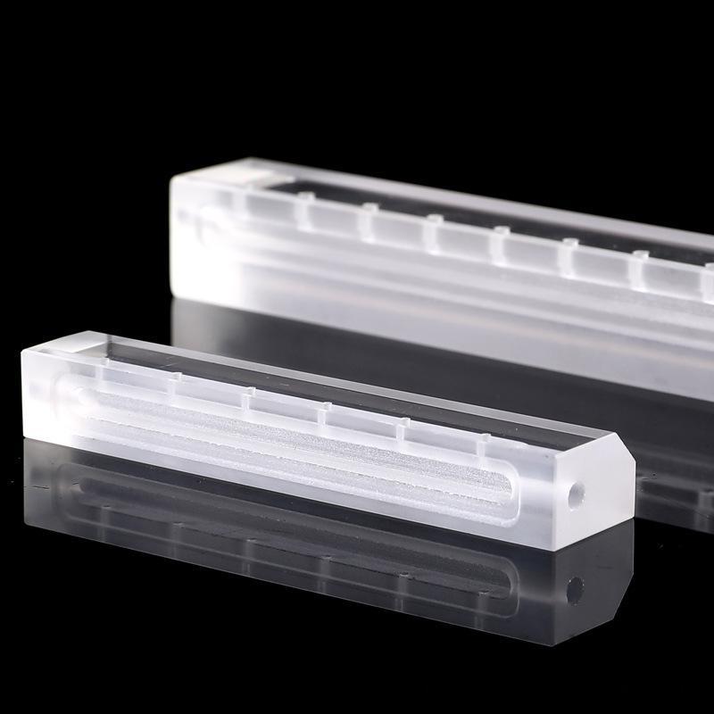
- Thickness: Ultra-thin 0.1mm - 2.0mm
- Surface Roughness: Ra < 0.5 nm CMP
- Transmittance: >92% (UV-VIS-NIR)
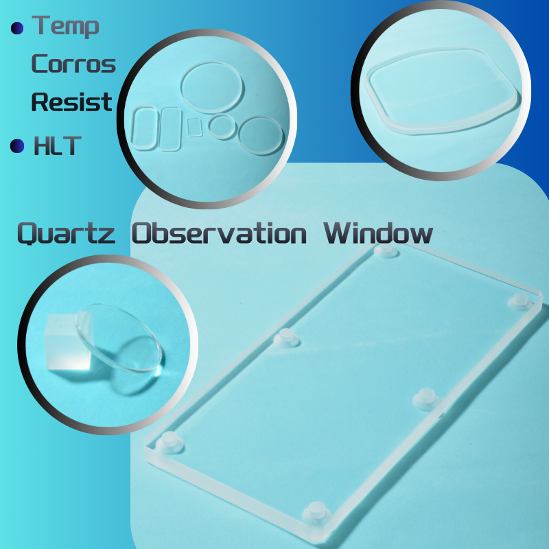
- Purity: 99.99% - 99.999% SiO₂
- Mohs Hardness: 5.5 - 6.5
- Max Working Temp: 1100°C - 1450°C
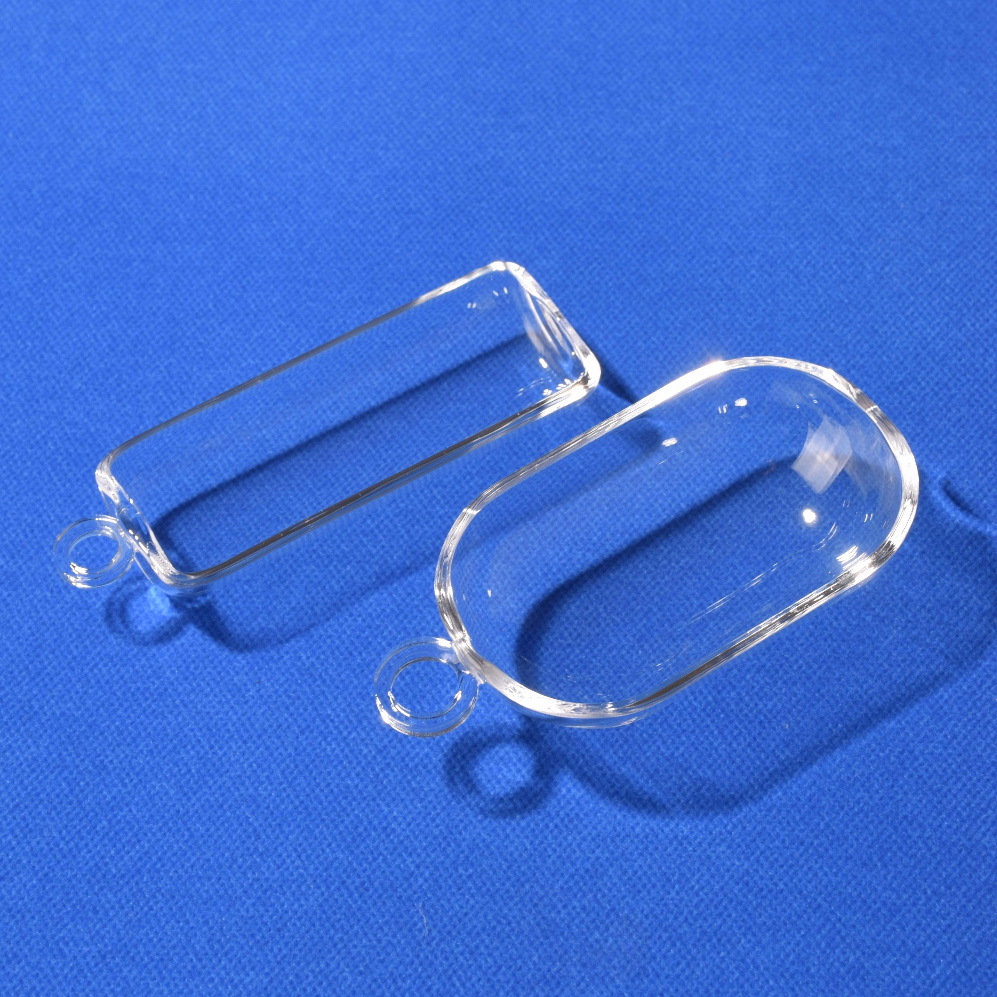
- Form: Semi-circular Flat Bottom
- Optical Quality: Bubble-free Class 0/I
- Fire Polishing: Oxy-hydrogen sealed
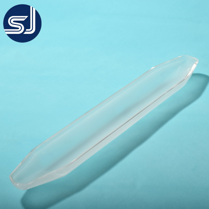
- Application: Diffusion & CVD Carrier
- Wafer Slots: Custom 25/50 Pitch
- Softening Point: 1683°C
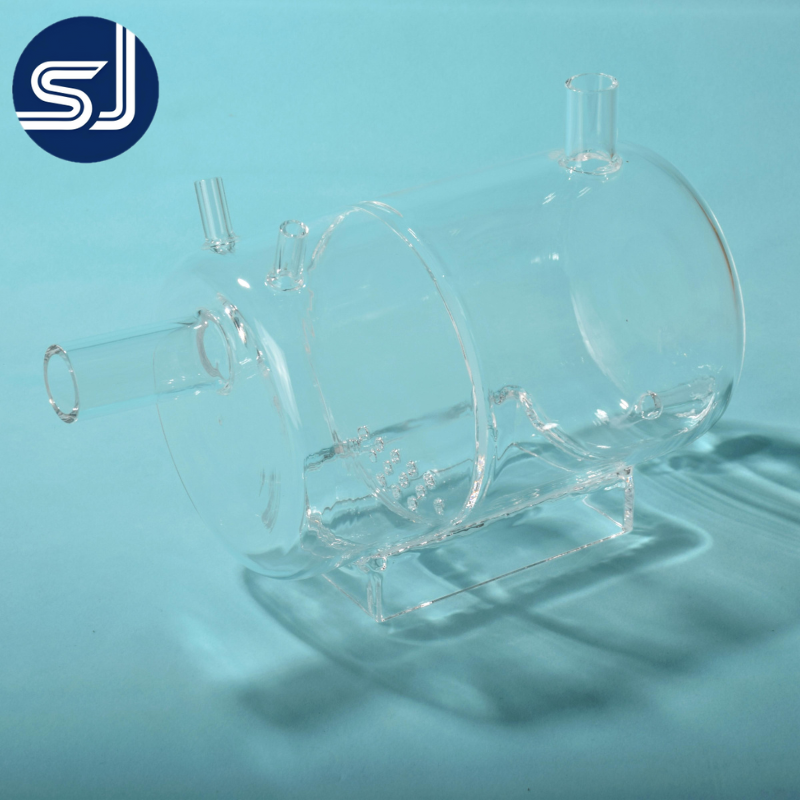
- Acid Resistance: 30x higher than ceramic
- Joint Tolerances: Ground Standard Taper
- Thermal Shock: ΔT = 1100°C to Cold Water
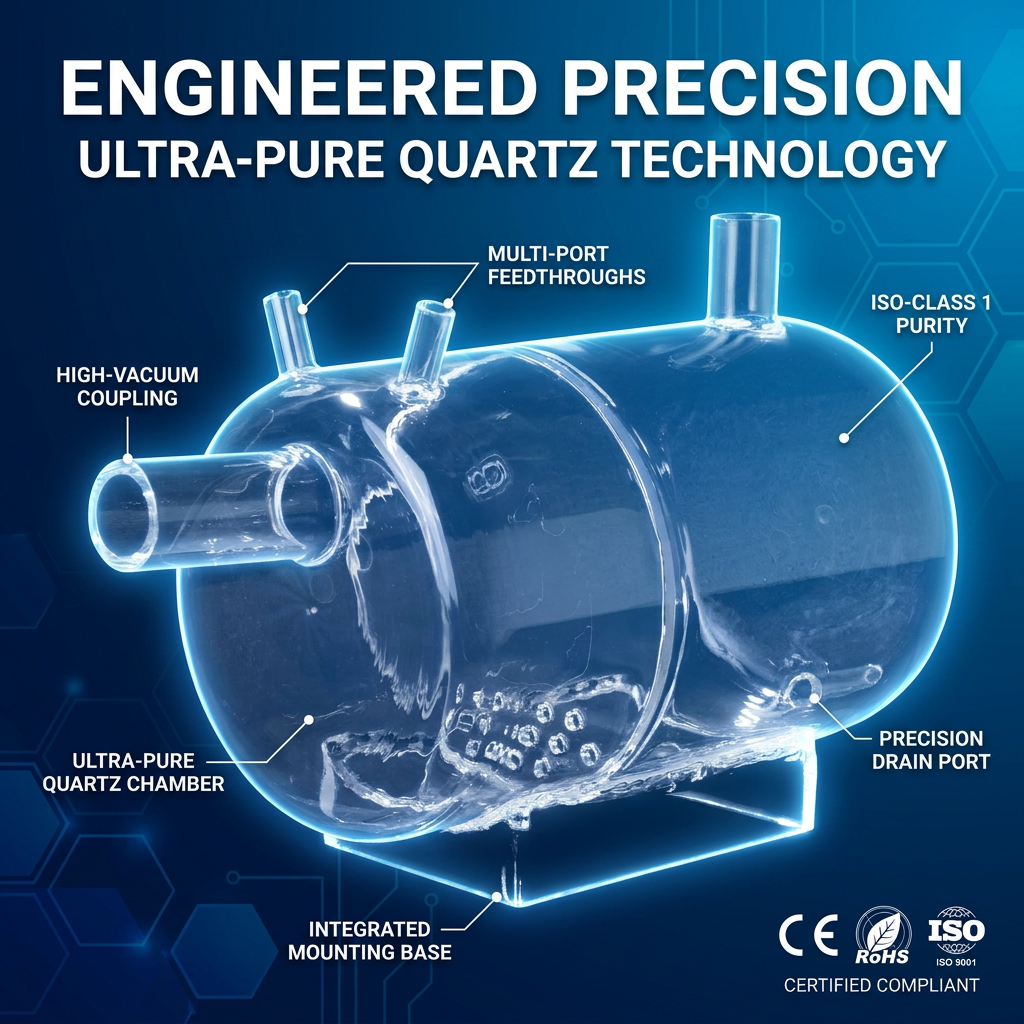
- Trace Element: Fe < 0.2 ppm, Al < 8 ppm
- Cleanroom Cleaned: Class 1000 DI Flush
- Custom Ports: Flanged / Threaded / Luer
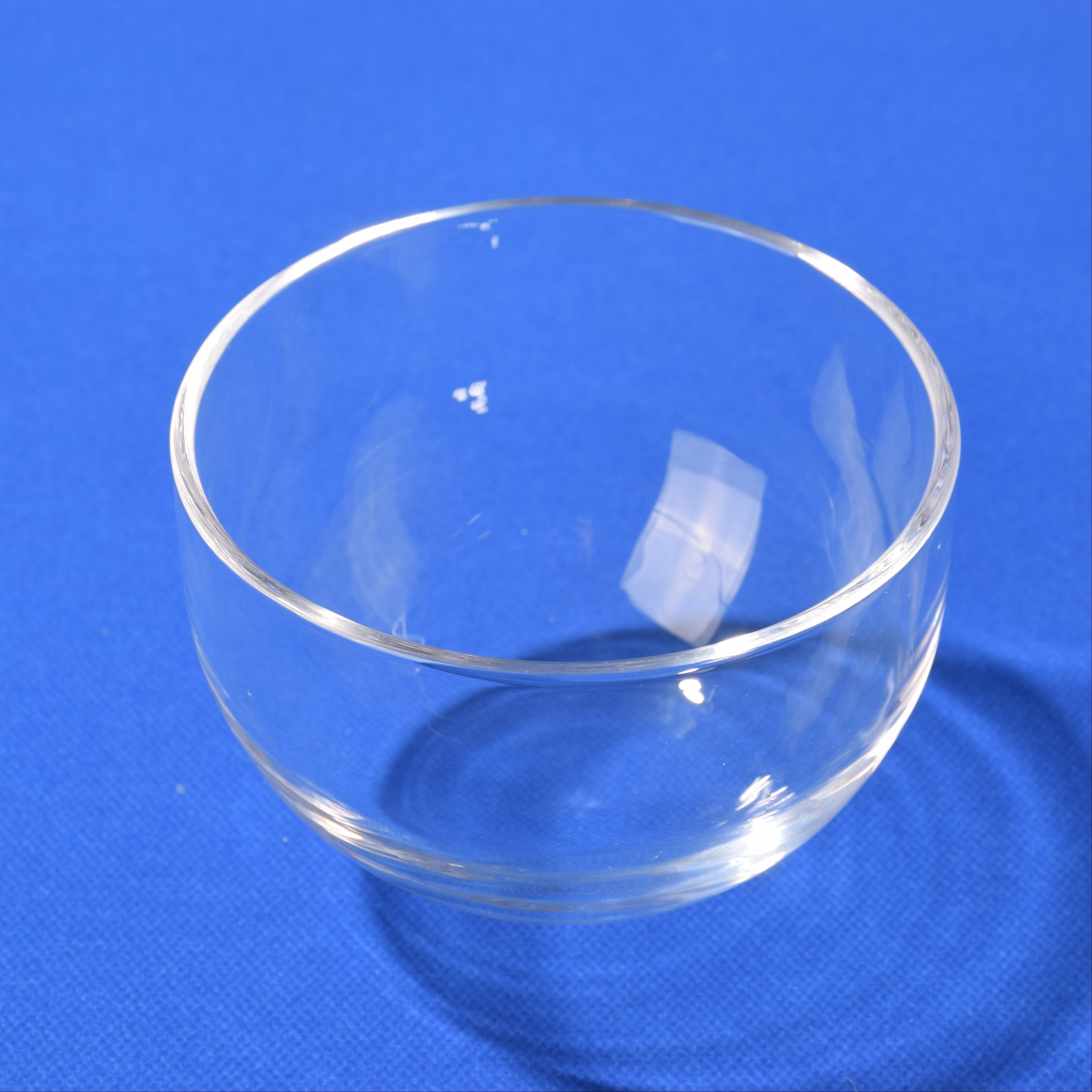
- Tensile Strength: 48 N/mm²
- Softening Point: 1683°C (Anneal: 1215°C)
- Crucible Volume: 10ml to 5000ml custom
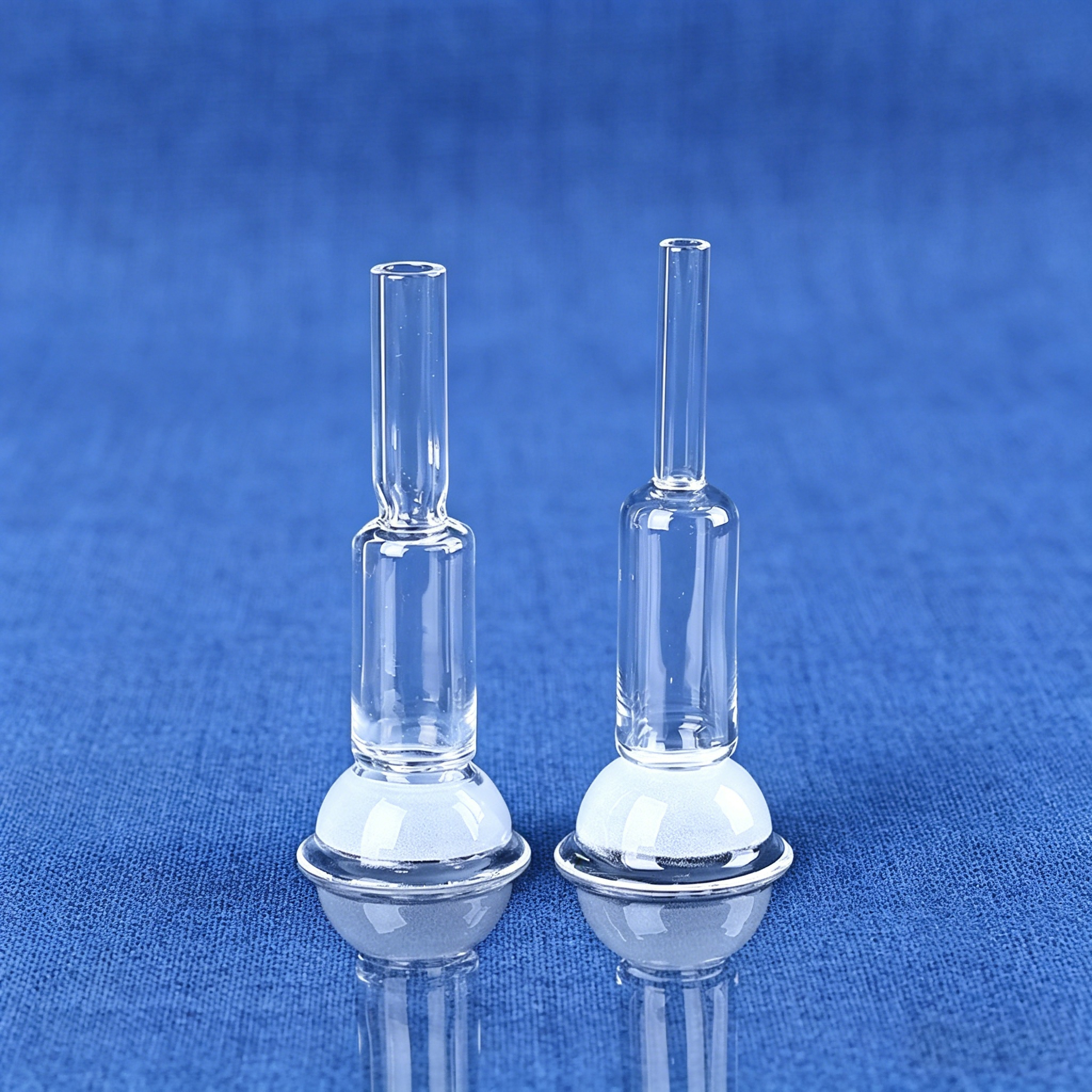
- Form: Precision C-Shaped Bending
- Standard Compatibility: Quantachrome / Micromeritics
- Vacuum Integrity: Helium Leak < 1x10⁻⁹ mbar·l/s
Ultra-low elemental trace contamination for advanced semiconductor and EUV lithography.
Double-sided chemical mechanical planarization (CMP) delivering atomic-scale flatness.
Exceptional thermal shock endurance capable of withstanding instant 1100°C quenching.
Flexible OEM/ODM engineering validation backed by complete CMM metrology inspection.
Engineering White Paper: Material Science of Fused Quartz & Synthetic Silica Plates
In high-precision manufacturing, optical metrology, and semiconductor fabrication, selecting the correct substrate is the defining factor in determining thermal deformation, transmission loss, and plasma etch longevity. While the term "quartz plate" is often utilized as a generic descriptor, material scientists and optical engineers categorize these vitrified vitreous silica products into distinct metallurgical and optical categories: Natural Fused Quartz (JGS2), Synthetic Fused Silica (JGS1), and Infrared Optical Quartz (JGS3).
1. Optical Grade Stratification: JGS1 vs. JGS2 vs. JGS3
For procurement officers and R&D directors, specifying the correct ISO/DIN grade ensures design-intent fidelity without unnecessary budgetary inflation. The optical and chemical variances are summarized below:
| Standard Grade | Material Synthesis Route | Useful Spectral Range | Typical OH Content | Primary Industrial Applications |
|---|---|---|---|---|
| JGS1 (Synthetic Silica) | SiCl₄ + O₂ Chemical Vapor Deposition | 185 nm – 2500 nm (Deep UV) | < 5 ppm to > 1200 ppm (Grade dep.) | Excimer laser windows, lithography mask blanks, DUV lenses, wafer inspection |
| JGS2 (Optical Fused Quartz) | Oxy-hydrogen Flame Fused Natural Sand | 220 nm – 2500 nm (UV-VIS-NIR) | 150 ppm – 300 ppm | Optical sight glasses, high-temp observation windows, semiconductor furnace plates |
| JGS3 (Infrared Fused Silica) | Vacuum Electric Fusion Natural Quartz | 260 nm – 3500 nm (Infrared Trans.) | < 5 ppm (Water-free) | IR analytical prisms, pyroelectric sensors, CO₂ laser optics, thermal viewports |
2. Trace Element Impurities: GDMS Analysis (PPM by Weight)
In sub-7nm node semiconductor wafer chucking, epitaxial deposition, and atomic layer etching (ALE), volatile alkali and transition metals trigger catastrophic gate oxide breakdown. Our factory implements high-purity natural silica sand sourced directly from the Donghai mineral belt, purified through acid leaching, flotation, and vacuum calcination to meet rigorous semiconductor fab criteria:
| Element Impurity | Aluminum (Al) | Iron (Fe) | Calcium (Ca) | Sodium (Na) | Potassium (K) | Lithium (Li) | Titanium (Ti) |
|---|---|---|---|---|---|---|---|
| Standard Clear Plate | 14.0 ppm | 0.8 ppm | 0.6 ppm | 1.2 ppm | 1.0 ppm | 0.8 ppm | 1.8 ppm |
| High-Purity 4N8 Grade | 6.5 ppm | 0.15 ppm | 0.3 ppm | 0.3 ppm | 0.2 ppm | 0.2 ppm | 0.8 ppm |
| Semiconductor 5N Grade | < 3.0 ppm | < 0.05 ppm | < 0.1 ppm | < 0.05 ppm | < 0.05 ppm | < 0.05 ppm | < 0.2 ppm |
3. Precision Sub-Nanometer Polishing & Dimensional Metrology
A pristine raw quartz ingot requires sophisticated double-sided chemical mechanical planarization (CMP) to eliminate micro-cracks, Sub-Surface Damage (SSD), and high-frequency spatial waviness. As a specialized OEM/ODM exporter, our manufacturing floor operates within ISO Class 6 cleanroom parameters, utilizing synthetic pitch polishers, cerium oxide (CeO₂), and colloidal silica slurries.
Surface Flatness (Wavefront)
Interferometrically verified up to λ/10 @ 632.8 nm across the entire Clear Aperture (CA > 90%), preventing distortion in laser beam splitters and interferometer reference flats.
Surface Quality (MIL-PRF-13830B)
Achieving 20-10 or 10-5 Scratch-Dig standards under high-intensity dark-field inspection, ensuring complete freedom from pinholes, inclusions, and sleek defects.
Parallelism & Wedge Error
Controlled within < 5 arcseconds (0.025 mm TTV) using laser autocollimators, essential for ultra-thin testing sheets, XRD zero-background holders, and laser windows.
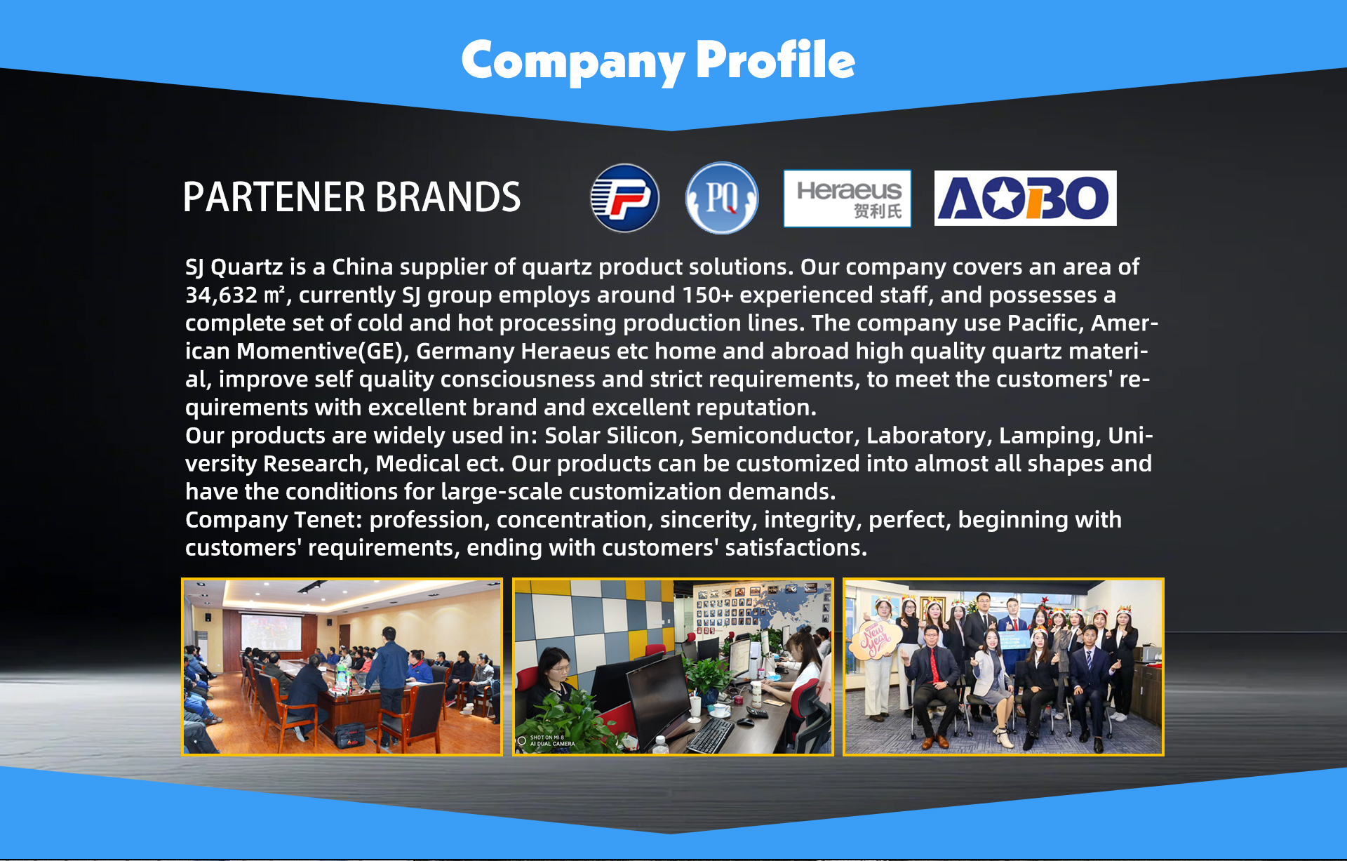
Full-Cycle Cold Machining & Hot Working Facilities
From custom 0.1 mm thin circular inspection discs to massive 800 mm diffusion furnace quartz plates, our factory integrates every phase of fabrication.
Multi-Axis CNC Machining
Diamond-tooled ultrasonic CNC milling, step-milling, contour edging, and waterjet profiling with positional tolerances held within ±0.01 mm.
Oxy-Hydrogen Lathes
Thermal flame bending, precision tube-to-plate fusion welding, and flange sealing handled by master glassblowers with 15+ years of craft expertise.
Thermal De-Stressing (Anneal)
Computerized continuous electric annealing lehrs soaking quartz at 1215°C to eliminate residual stress birefringence below 5 nm/cm.
Acid Etching & Cleanroom Pack
Ultra-pure HF/HNO₃ surface acid polishing followed by 18.2 MΩ·cm DI water ultrasonic bath cleaning and Class 1,000 double-vacuum pouch packing.
Future Procurement & Technological Trends in Fused Quartz
As microelectronics nodes migrate toward 2nm GAA (Gate-All-Around) architectures and high-power industrial lasers surpass 20kW CW, quartz substrate procurement demands are undergoing transformative technical shifts.
1. Shift to Angstrom-Level Roughness (Ra < 0.2 nm)
Standard semiconductor lapping (Ra ~ 0.8 nm) is becoming obsolete for extreme ultraviolet (EUV) optical components and pellicles. Global procurement mandates Magnetorheological Finishing (MRF) and Ion Beam Figuring (IBF) to eliminate scatter losses in 13.5 nm optical paths.
2. Ultra-Thin Substrates for Microfluidics & PICs
Optical quartz plates with thicknesses down to 50µm – 100µm are experiencing double-digit procurement growth. These serve as thermal dissipation carriers and bio-compatible flow channels for high-throughput DNA sequencing and photonic integrated circuit (PIC) interposers.
3. Direct OEM Factory Audits & Traceability
B2B procurement directors are abandoning trading intermediaries in favor of authenticated Source Factories verified by third-party testing institutions (TÜV, SGS). Tier-1 manufacturers must supply GDMS trace element analysis, laser interferometer certificates, and ISO cleanroom validation for every production lot.
Technological Evolution: The Next Decade of Quartz Plate Manufacturing
The global fused silica market is moving beyond simple mechanical glass cutting. Below is the technical roadmap shaping precision manufacturing through 2030:
Green Chemical Mechanical Planarization (CMP): Closed-loop hydrofluoric acid recovery systems and bio-degradable slurry chemistries are replacing caustic legacy abrasives in response to stringent ESG and carbon-neutrality supply mandates in the EU and North America.
Laser Damage Threshold (LIDT) Optimization: Advanced pulsed laser applications (Femtosecond and Picosecond machining) require polished quartz plates capable of enduring pulse energies > 15 J/cm² @ 1064 nm, 10 ns. By eliminating subsurface micro-fissures via proprietary HF etching and laser-driven fire polishing, thermal lensing and beam distortion are completely suppressed.
Large-Aperture Monolithic Growth: As flat panel displays (OLED/micro-LED) and semiconductor wafer carriers expand to 300 mm and 450 mm standards, continuous electric arc fusion techniques now enable massive polished quartz sheets exceeding 1200 mm × 1000 mm without bubble coalescence or devitrification centers.
Frequently Asked Questions: Polished Quartz Plate Procurement
Technical guidance direct from our chief process engineers to assist international buyers, metrology labs, and procurement specialists.
What is the maximum continuous working temperature of your polished quartz plates?
How do I select between JGS1 (Synthetic Silica) and JGS2 (Fused Quartz) for my application?
What surface roughness and flatness tolerances can your polishing facility guarantee?
What is the Minimum Order Quantity (MOQ) for custom-dimension quartz plates?
How do you safeguard ultra-thin and large-format quartz plates against breakage during overseas shipping?
Can you provide third-party metallurgical inspection and optical testing certificates?
How resistant is fused quartz to corrosive acids and alkaline solutions?
Launch Your Custom Quartz Plate Project Today
Whether you require 1-piece R&D prototyping with custom CNC beveling, laser testing substrates, or recurring batch supplies of semiconductor-grade fused quartz plates, our Donghai engineering team provides drawing reviews within 12 hours.
Send an Inquiry